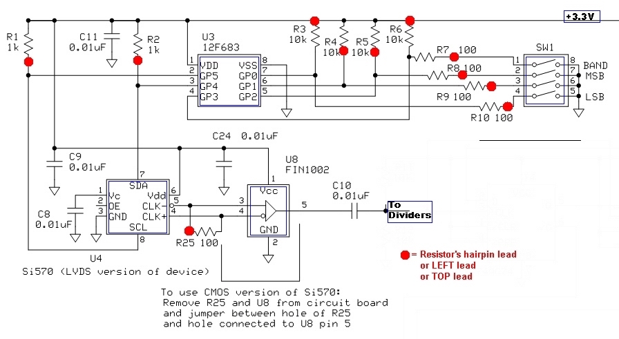
Schematic
Theory of Operation
The local oscillator (U4)is a programmable oscillator, whose programmatic parameters
are set by the microcontroller, U3. U3 is programmed with 16 different values corresponding
to the settings of dip switch SW1. Without U3 in the circuit, U4 would default to
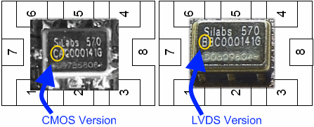
an output frequency of 56.320 mHz. The IC U8 is needed if the version of U4 is the
"LVDS" version. If U4 is a CMOS version, U8 (and R25) is not required and, instead
a jumper wire is installed to bypass them.
This LO stage must produce an output RF signal that is four times the desired center
frequency for the radio. This is then fed to the dividers section to produce the
two center-frequency signals that are in quadrature.
Summary Build Steps
- Install U8 (ignore if Si570 is CMOS)
- Install U4
- Install the 4 SMT Caps
- Install SW1
- Install the resistors (ignore R25 if Si570 is CMOS)
- Install Sockets J1 and J2
- Install C10
- Install U3 socket, then plug in U3
- Testing
Bill of Materials
| Designation | Component | Type | Qty | Notes |
|---|---|---|---|---|
| C08 | 0.01 µF | SMT 1206 | 1 | |
| C09 | 0.01 µF | SMT 1206 | 1 | |
| C10 | 0.01 µF | ceramic | 1 | code 103 |
| C11 | 0.01 µF | SMT 1206 | 1 | |
| C24 | 0.01 µF | SMT 1206 | 1 | |
| J1 | 2-pin socket | socket for BPF board P1 | 1 | Install before C10 |
| J2 | 3 pin socket | socket for BPF board P2 | 1 | Install before C10 |
| R01 | 1k Ohm | Resistor 1% | 1 | hairpin (north-south) |
| R02 | 1k Ohm | Resistor 1% | 1 | Hairpin (south - North) |
| R03 | 10k Ohm | Resistor 1% | 1 | Hairpin (south - North) |
| R04 | 10k Ohm | Resistor 1% | 1 | hairpin (north-south) |
| R05 | 10k Ohm | Resistor 1% | 1 | hairpin (north-south) |
| R06 | 10k Ohm | Resistor 1% | 1 | Hairpin (south - North) |
| R07 | 100 Ohm | Resistor 1% | 1 | hairpin (east- west) |
| R08 | 100 Ohm | Resistor 1% | 1 | hairpin (east- west) |
| R09 | 100 Ohm | Resistor 1% | 1 | hairpin (east- west) |
| R10 | 100 Ohm | Resistor 1% | 1 | hairpin (east- west) |
| R25 | 100 Ohm | Resistor 1% | 1 | flat - ignore for CMOS SI570 |
| SW1 | 4-pos dip switch | 8 pin Dip Switch | 1 | |
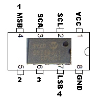
| U3 | 12F683 | CPU and socket | 1 | (top) |
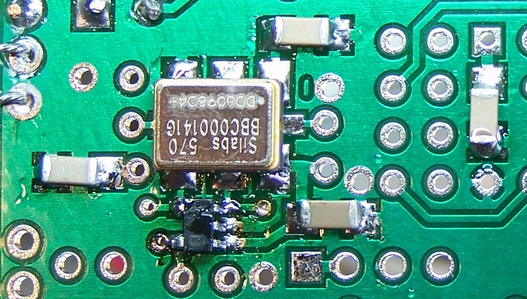
| U4 | Si570 LVDS | Oscillator | 1 | (bottom) |
| U8 | FIN1002 | Diff LVDS Rcvr | 1 | (bottom) |
Installation Notes
Bottomside Components
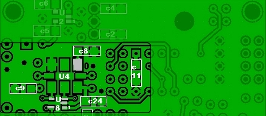
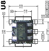
Mount U8
. Note: if the kit is a CMOS SI570, then do NOT install U8. Take ESD precautions. See the guide for mounting SMT ICs.- (For the LVDS kit version only) mount U8 (see table below for orientation) Take great care mounting U8. It is very tiny and mounts just below pins 4 and 5 of U4. This is an area that is very ripe for solder bridges!
- Carefully check the soldering of U8, especially around pin 2 (the ground connection) and pin 5 (VCC). You do not want to short 5Vdc to ground at that point!
- A good post-soldering test on U8 is to check the resistance between U8 pin 1 and ground. If it is low, you have a soldering problem.
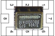
Mount U4
.- Mount U4 (see table below for orientation) - note: author's kit was an LVDS version
- Note: please note that U4 has 8 pins (7 and 8 are at either end of the chip).
- Also note that you will be installing the IC on the bottom of the board such that the writing on the chip is upside down with respect to the top edge of the board.
| Check | Designation | Component | Orientation |
|---|---|---|---|
| U8* | FIN1002 (code="FN02X") |
|
|
| U4 | Si570 LVDS |
|
Mount the 4 SMT Capacitors
- Mount .01 µF capson the underside of the board (see guide for mounting SMT Capacitors). )
- Note that all are from the set of ten 0.01 µF caps (no 0.1 µF caps).
| Check | Designation | Component |
|---|---|---|
| C08 | 0.01 µF | |
| C09 | 0.01 µF | |
| C11 | 0.01 µF | |
| C24 | 0.01 µF |
Topside Components
SI570 - CMOS vs. LVDS
-
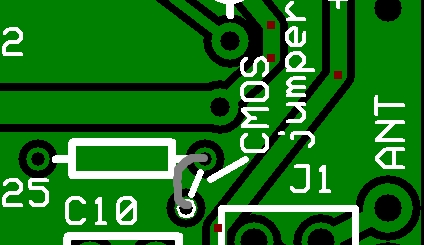
- If the kit is a CMOS version:
- Do NOT install R25 and U8
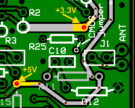
- Instead, install a jumper wire between the hole of R25 and the hole connected to U8-Pin5. You should use a very fine wire for the jumper, as the holes for it are quite small in diameter. In addition, you should install the jumper wire as a topside component (i.e., do not try to install the wire to the bottomside - thanks to Pete N4ZR for this suggestion). Reference the illustration below:
For a discussion of SI570's versions and the need for the FIN1002, see see the analysis by J. K. DE Marco PY2WM.
Topside Layout
Mount SW1
-
Mount the 8 pin Dip Switch. Orient the switch such that the numbers
(1, 2, 3, 4) are closest
to the right hand edge of the board and read, in their ordinal sequence,
from
top to bottom.1.
- This switch provides a means to select one of 16 "center" frequencies, depending upon the settings for SW1.
| Check | Designation | Component | Orientation |
|---|---|---|---|
| SW1 | 4-pos dip switch |  |
1 If you accidentally mount SW1 backwards (as the author did on the first go around), all is not lost. The switches will still work; you'll just have to remember that the MSB corresponds to switch #4 and the LSB corresponds to #1 when dialing in the frequency "nibbles".
Mount the 11 resistors
(see the guide to mounting resistors)- Mount the 10 hairpin resistors, R1 thru R10 (see table below for orientation)
- (For the LVDS kit version only), Mount R25 (mounted flat). This step does not apply if the kit is the CMOS version.
| Check | Designation | Component | Orientation | Notes . |
|---|---|---|---|---|
| R01 | 1k Ohm | hairpin (north-south) | ||
| R02 | 1k Ohm | Hairpin (south - North) | ||
| R03 | 10k Ohm | Hairpin (south - North) | ||
| R04 | 10k Ohm | hairpin (north-south) | ||
| R05 | 10k Ohm | hairpin (north-south) | ||
| R06 | 10k Ohm | Hairpin (south - North) | ||
| R07 | 100 Ohm | hairpin (east- west) | ||
| R08 | 100 Ohm | hairpin (east- west) | ||
| R09 | 100 Ohm | hairpin (east- west) | ||
| R10 | 100 Ohm | hairpin (east- west) | ||
| R25* | 100 Ohm | flat - ignore for CMOS SI570 |
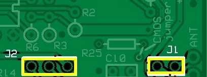
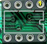
Mount BPF Board Sockets, J1 and J2
Mount the 2-pin and 3-pin sockets on the topside (J1 and J2) with the ends going down through the holes in the main board(1)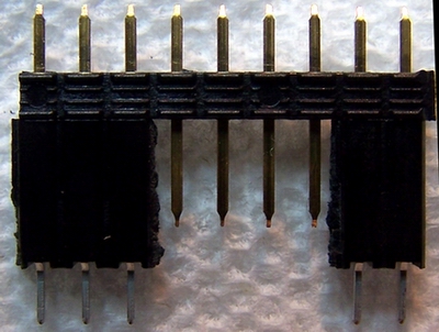
- Use the 9-pin header piece provided in the kit to align sockets J1 and J2 to ensure a good fit with the header pins on the BPF boards (see later instructions on BPF Boards).
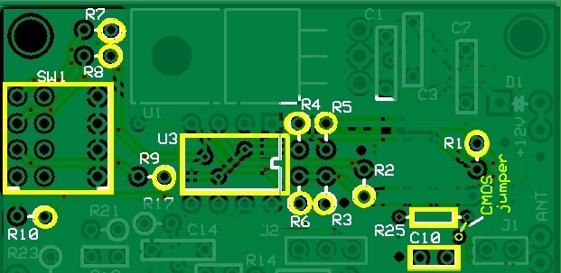
- Note: These need to be mounted before C10, so that this header pin alignment method can be used without C10 interfering with the "bridge" (see photo above).
Mount C10
- Mount the ceramic capacitor C10 (see guide for mounting ceramic capacitors)
| Check | Designation | Component |
|---|---|---|
| C10 | 0.01 µF (code 103) |
Mount CMOS Jumper (if Si570 is CMOS version)
- If the Si570 version is CMOS, install the CMOS jumper wire as ingicated in the graphic above.)
| Check | Designation | Component |
|---|---|---|
| CMOS jumper wire | (use cut-off resistor lead) |
Mount the socket for U3
- The socket should be oriented so that the notched end is on the right (be careful placing the pins correctly
- "measure twice, cut once")
Plug U3 into its socket
- Take ESD precautions when handling U3
- Take care to match the notch correctly.
| Check | Designation | Component | Orientation |
|---|---|---|---|
| U3 |
12F683
(topside)
|
|
Completed Stage Board
Top
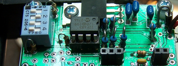
Bottom
Testing
Current Limited Power Test
- Connect a 100 ohm resistor in series with the power line and apply 12 V dc power
- the current should be relatively low (around 10 mA or less)
- Measure the voltage WRT ground at the +5 V and at the 3.3 Vdc testpoints.
- A voltage of around 2 V dc on each testpoint indicates the power rails are not shorted
Current Draw (DMM - 93 mA)
- Current draw here is for the LVDS version of the Si570. Adjust these numbers down by about 14 mA for the CMOS version.
- The current draw should be somewhere between 80 and 100 mA. The exact value is very much dependent upon the Si570, the version (CMOS vs LVDS), the frequency setting, and component variations in the circuit.
- You can try measuring the current draw for various SW1 settings to see the effect of frequency on current draw.
- If you get these results, and the power rails are at/near 3.3V and 5.0 V dc, respectively, then you are doing fine and can move on.
SW1/U3 Tests (DMM - 3.3 Vdc, 33 mVdc)
You can test the SW1 programming of U3 by checking the dc voltages at pins 1 thru 7. Pins 1 thru 3 should always be approximately 3.27 Vdc. Voltages at pins 4 thru 7 will vary, depending upon their corresponding dip switch settings (pins 4 thru 7 correspond to dip switches 1 thru 4):.
- When the switch is ON, the corresponding voltage drops to LOW (~33 mV).
- When the switch is OFF, the corresponding pin's voltage is HIGH (~3.27 V).
- If the voltages are not as expected, remove U3 from its socket and retest to ensure that the SW1/U3-Socket wiring is good.
- In this case, if the tests are passed with U3 removed, you should suspect U3.
Frequency Test
- Set the SW1 switches for 7.046 MHz, as above
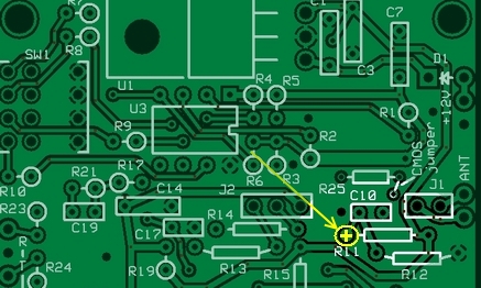
- Connect a clip lead to the left-hand lead of R11 (to act as an "antenna" for the Si570's signal)
- Connect a wire to your transceiver's RX ANT jack lay it in proximity to the clip lead to loosely couple the signal
- Power up the transceiver and tune it to 28.184 MHz
- Power up the board. You should hear the signal on your transceiver.
LO Output (Scope/Freq Counter)
The Local Oscillator should output a signal at the four times the center frequency selected by the switch settings of SW1.
Test
:- Set the switches of SW1 to 0100 to get a center frequency of 7.046 MHz
- (See Sw1 Switch Settings)
- Apply power to the board
- Test the output of (U8 in the LVDS version of the kit or U4 in the CMOS version)
at the left-hand lead of R11 (or Pin3 of U5): the frequency should
be 28.184 MHz (4 times the desired center frequency of 7.046 MHz).
The AC pk-pk voltage should be aproximately equal to or less than 3.3 V p-p. - If you get 56.32 MHz (or 14.08 times 4) with SW1 set as above, or regardless
of SW1 settings, this means:
- that U3 has not been installed or
- U3 has been incorrectly installed or
- pins 7 or 8 of U4 may have bad solder joints