Welcome to the G40 Experience
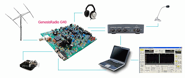
Welcome to my G40 website. I have built these pages to document and trace my experience in building the new Genesis G40 40m SDR 5W QRP Transceiver. This radio was designed by Tasic Sinisa (Tasa YU1LM), in Belgrade, Serbia, and is documented, kitted and shipped by Nick Hacko VK1AA, in Sidney Australia. I have no commercial interest in the G40 or its creators. In the interests of full disclosure, it should be pointed out that I did receive my G40 as a courtesy in return for providing the documentation herein. Elsewhere on the WB5RVZ site, I have documented my construction of the various Softrock SDR kits. The new Genesis Radio line is very interesting departure from the Softrocks in many respects:
- First, I will not be providing extensive "Heathkit-like" builders notes for the G40 - the work that Nick Hacko VK1AA of GenesisRadio has done on documenting these is first rate and needs little if any augmentation. It does, however, need some aggragation, in that there are multiple sources of guidance. Perhaps my efforts herein can provide a single, authoritative resource for the builder.
- Second, the kit does not involve SMT components. Many builders are put off by SMT (although many I have coaxed through the first few chips have later confessed that the issue is really overblown). However, for the faint of heart, this kit shields the builder from SMT
- Finally, while there is coil winding, the few inductors that must be wound are quite easily constructed and are of a size and shape that are pleasantly comfortable for those of us of limited dexterity and eyesight.
I will likely follow up on this build with the G20 (not yet shipping) 20m kit and top it all off with the (TBD) G59 multiband transceiver kit.
Addendum here: just learned of neat site by Dusan YT1DL providing a tutorial on how to run various digital modes with SDR like G40.
TX ES 73
DE Robby WB5RVZ
In the Beginning
Kit Arrival
The kit arrived in a well-packed airmail box. Packed in it was a letter from GenesisRadio telling me that my G40 Version 1.0 number was "059", suggesting that 58 stalwarts preceded me in this journey. The letter also provided links to the Parts Inventory List, the Assembly Manual, and the OnLine Assembly Pictorial.
In addition to the letter, there was the PCB board and several envelopes of parts, by inventory category:
- Capacitors
- Resistors
- Inductors/Quartz
- Semiconductors and ICs
- Miscellaneous Parts and Hardware
Inventorying the Components
Nothing challenging here, other than the tedium. Being one to like a little order in the process, I took the parts list out of the downloaded document and converted it into an Excel Spreadsheet. In the spreadsheet, I organized the parts further into a Pivot Table allowing me to list out the parts for a specific bag/category and check them off to be sure all was there. Later, I will use the same pivot table to list the parts out by each of the 8 phases in the build, organizing them into phase-specific bags O' parts.
Reviewing the Instructions/Schematics
First thing I notice is that there are some slight disconnects between the liberally illustrated, online assembly pictorials (with associated instructions) and the Word Document of the Assembly Manual. For example, Phase 1 calls for 21 diodes plus a zener diode. These are referenced in the online docs, but not in the word document. My customary practice of breaking the schematic out by phase is likely not going to work for me with this kit. Still, everything is all there; just spread out a bit. Lesson to be taken away from this is to thoroughly review the instructions (all versions: Word, on-line, and BOM) for each phase before beginning construction in that phase. You want to know what you are doing with each component and where on the board!
Checking out the Schematics - Oops!
Before going into a build, I always like to familiarize myself with the schematics and make sure I can track from the schematic to the PCB and vice versa. The documentation provided on the website (Word Document) has 4 bits of schematic which are apparently snapshots of development as the design progressed (or intended for general purpose use in the follow-on kits). Unfortunately, at least for me, this made it quite difficult to track from the schematic to the PC and back, since the identifiers (e.g., "R9", "C53", "L4", etc.) of most of the components in the schematics did not match with the identifiers on the silk-screen. Of course, one could always reverse engineer the PCB back to the schematic by essentially repeating the schematic-to-pcb mapping process in reverse. I am not up to that task and have asked GenesisRadio if it might be possible to publish a complete schematic that agrees on component identifiers with the pcb silkscreen. This would make any required troubleshooting (not that I expect to need any) infinitely easier.
Virtual Build
When I encounter a new kit and a new design, I like to go through a "virtual build" - virtually placing components onto an image of the board, stage-by-stage. This forces me to devote the time and effort to really understand the circuit(s) and also provides materials for use in enhanced documentation of the kit and its construction. This turns out to be particularly valueable in the case of the G40 because there are potential ambiguities brought about by the schematic segmentation and inconsistent component identification mentioned above.
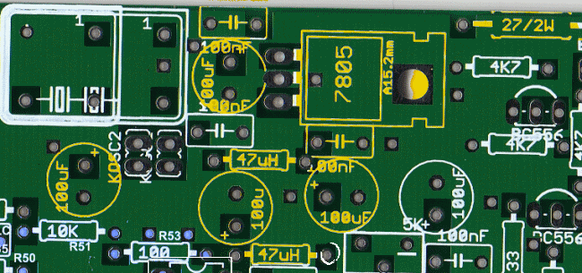
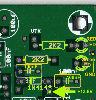
Phase 01: Virtual Power Supply and Sundry Diodes
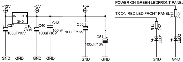
The purpose of this stage is to provide the 5 Volt power rail for the CMOS ICs (as well as provide for Power and TX LEDs and the 12 Volt input point. Make sure your external power supply has the correct volatge (12-13.8 Vdc) and it should be capable of producing 2 to 3 Amps. A faulty or underrated power supply is a very common problem.
Schematic
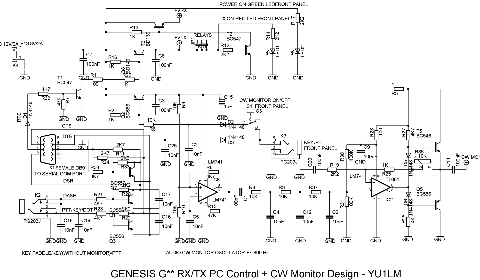
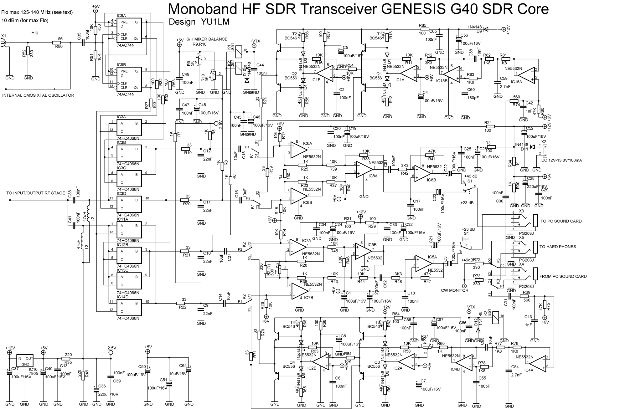
This stage had two areas of the board which were populated to provide the 5 V power supply and the LEDs for RX and TX. In addition, there were some diodes that were populated throughout the board (1 zener and 21 regular diodes). Parts of this stage are spread across two of the schematics: "Genesis G** RX/TX PC Control + CW Monitor Design" and "Monoband HF SDR Transceiver Genesis G40".
Below is a construction of a partial schematic for this stage (not all components are represented):
BOM
| Component | Qty |
|---|---|
| PCB G** | 1 |
| Diode Zen 1N4734 5.6V | 1 |
| Diode 1N4148 | 21 |
| LED Green | 1 |
| LED Red | 1 |
| Resistor 2.2 K 1/4W | 2 |
| Resistor 20 Ohm (27R) 2W | 1 |
| Capacitor 100 nF 104 MLC 50V | 4 |
| Cap. Electrolytic 100uF 25V | 4 |
| Volt. Stab. 7805 L7805CV | 1 |
| Choke 47uH | 2 |
Parts Placement
The 21 diodes and their placement were, to borrow a phrase, "all over the board" - literally:
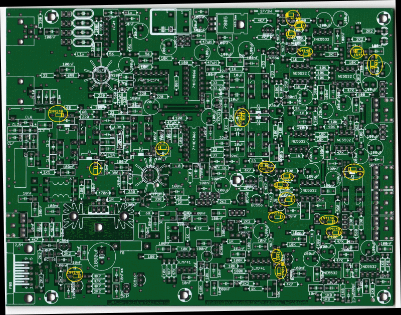
The remaining single zener diode was placed:
Power Supply Testing
Temporarily connect a +12V to +14V power supply at the "13.8V" and "GND" connection points shown in the PCB layout above. The green LED should light up.
Measure the voltage on the 5V rail (pin 3 of LM7805) with respect to ground. You should see something on the order of 4.9-5.0 Vdc.
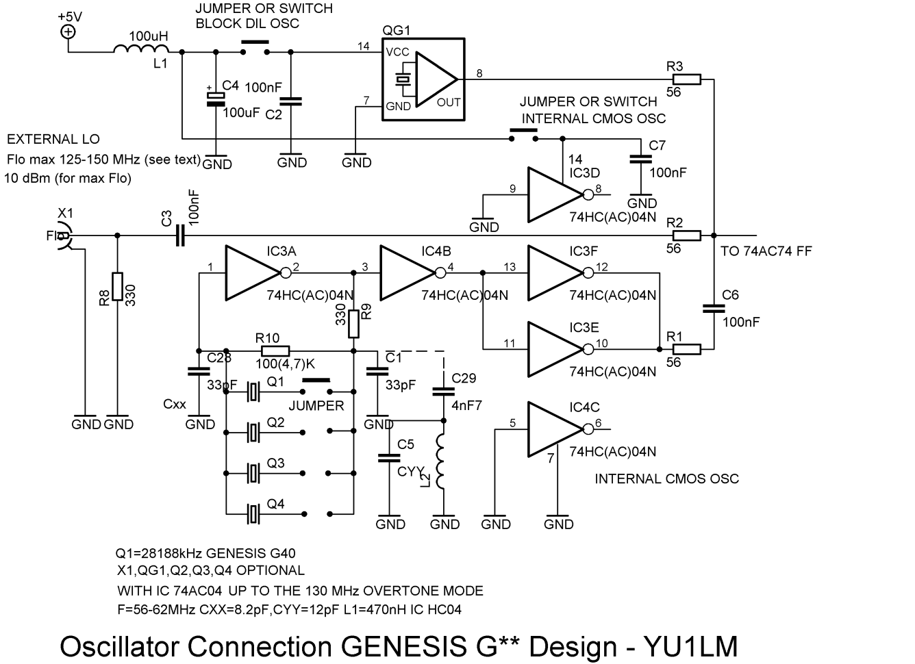
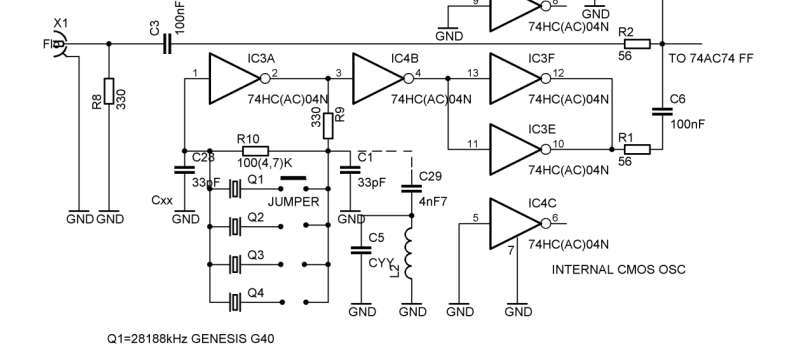
Phase 02: Local Oscillator
The local oscillator stage generates a 28.188 MHz signal (for quadrature clocking signals of 7.047 MHz each) using a 74HC04 hex inverter and a 21.188 MHz crystal. The circuit is described in the schematic "Oscillator Connection Genesis G** Design". The output of this stage will divided in the follow-on stage.
Schematic
BOM
| Component | Qty |
|---|---|
| Jumper wire (clipped off component leads) | 4 |
| Resistor 56 Ohm 1/4W | 3 |
| Resistor 330 Ohm 1/4W | 2 |
| Resistor 4.7 K 1/4W board shows 100K | 1 |
| Capacitor 100 nF 104 MLC 50V | 1 |
| Capacitor 10 nF 103 MLC 50V | 1 |
| Capacitor 33 pf Ceramic | 2 |
| Cap. Electrolytic 100uF 25V | 1 |
| BNC Connector (optional -X1 on schematic) | 1 |
| IC 74HC04 SN74HC04N Hex Inverter | 1 |
| Quartz Crystal 28.188MHz | 1 |
LO Parts Placement
Parts placment was fairly straight-forward and localized to the top left side of the board. The only potential point of confusion is the 100k resistor which is NOT used (a 4.7k resistor is used, instead):
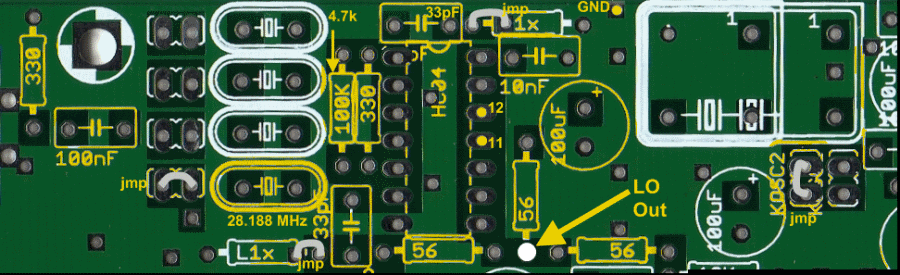
LO Testing
Voltages
Refer to above PCB layout for the two voltage testpoints
Connect the power supply as in Phase 1.
Check the voltage (with respect to ground) at pin 11 of the 74HC04 with the volt meter. It should read +1.5V to +3.9V.
Check the voltage (with respect to ground) at pin 12 of the 74HC04 with the volt meter. It should read +1.5V to +3.9V.
Otherwise if the voltage is close to 0 or +5V then the oscillator is not working correctly.
Frequency
If you have a frequency counter or HF transceiver, look for a signal around 28.188 MHz to verify that the oscillator is providing output.
If you have an oscilloscope, you can probe at the "LO Out" testpoint (see above) for the 28.188 MHz signal.
Phase 03: RX (Dividers, Tayloe Detector, Opamps)
This phase is a large one, taking the builder to a working RX in one stage. The stage can be broken down into sub-stages:
- Dividers
- Tayloe-like detector whcih samples and holds the incoming RF into 4 "phase slices", as clocked by the dividers, down-converting the RF to AF.
- RX OpAmps - four opamp chains that output, at the end, the 0 degree and 90 degree I and Q audio signals
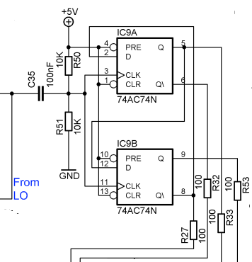
Dividers Sub-Phase
6 resistors, one capacitor, and one IC make up the divider, which breaks the LO signal into 4our components, each 1/4 the LO frequency and each separated in phase by 90 degrees:
Dividers Schematic
BOM
| Component | Qty |
|---|---|
| Dividers: | |
| IC 74AC74PC Dual D-FlipFlop | 1 |
| Resistor 10 K 1/4W | 2 |
| Resistor 100 Ohm 1/4W | 4 |
| Capacitor 100 nF 104 MLC 50V | 2 |
Parts Layout
Divider Testing
If you have a scope or frequency counter, you can test the operation of the divider sub-phase by powering up the board at 12 Vdc and probing the four pins: 5, 6, 8, and 9 on the 74AC74 chip. Each pin should register a frequency near 28.188/4=7.047 MHz. the wave forms should resemble those shown on the Mixer Schematic, below.
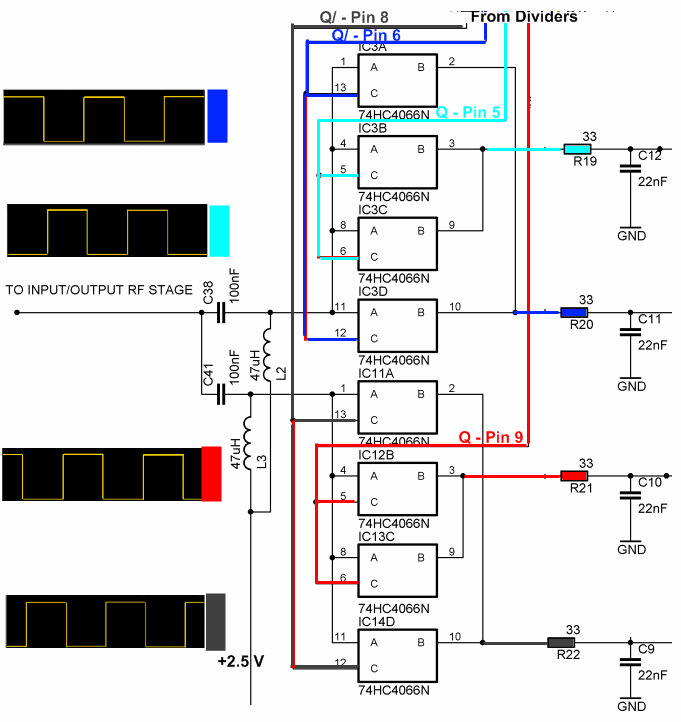
Mixer Sub-Phase
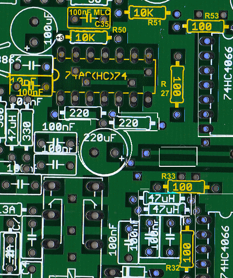
The G40's mixer is a double-balanced, sample and hold circuit using two quad bilateral analog switches (74HC4066), clocked by the four outputs from the dividers. Each pair of switches outputs to an RC pair that samples and holds the output for forwarding to the OpAmps Section. The portion of the schematic illustrating this is shown below (including divider output waveforms derived from a simulation of the divider operation). Not shown is that part of the circuit that uses two 5k trimpots for hardware balancing of the mixer.
The incoming RF is split into 2 streams, each going to two pairs of switches. Each switch pair is turned on and off by a signal coming from the dividers. The switched outputs of the pair are integrated by the corresponding RC circuit. As in theTayloe detector, the result is the down-conversion of the RF signals to their AF analogues. The resultant outputs of the mixers' RC circuits will go to the OpAmp chains to produce the I and Q audio signals for the PC.
Mixer Schenatic
BOM
| Component | Qty |
|---|---|
| Mixers: | |
| IC 74HC4066 Quad Bilteral Switch | 2 |
| Resistor 33 Ohm 1/4W | 4 |
| Resistor 220 Ohm 1/4W | 2 |
| Capacitor 100 nF 104 MLC 50V | 2 |
| Capacitor 22 nF 223J USM | 4 |
| Cap. Electrolytic 220uF 16V | 1 |
| Choke 47uH | 3 |
Parts Layout
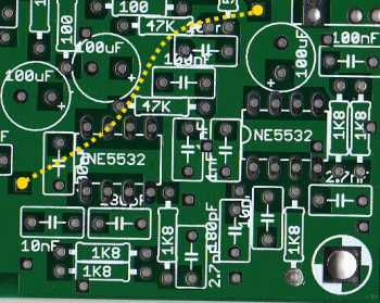
Here is the pcb area for the mixer:
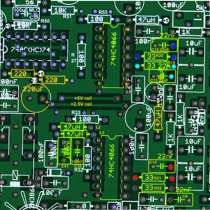
For Boards Serial Numbered from 1 to 100 ("VK6IC Fix")
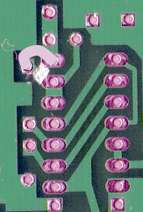
Boards numbered from 1 to 100 were shipped without on or more of the modifications in the pdf file describing the fix by VK6IC. This fix calls for cutting one trace and soldering a small jumper (both in the underside of the board, in the vicinity of pins 14 and 13 of the top 74HC4066 Quad Bilteral Switch IC. The original board design had pin 13 connected to a bypass capacitor. The modification removes that connection and makes a connection between pin 14 and the bypass capacitor. Some boards in the higher numbers of the 1-100 range have already had the trace cut but still need the jumper wire soldered, as in the case of the author's board:
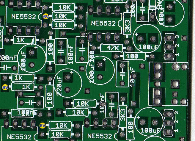
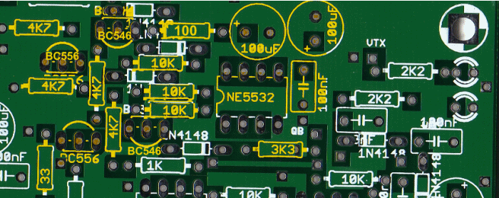
RX Opamps - Sub-Phase
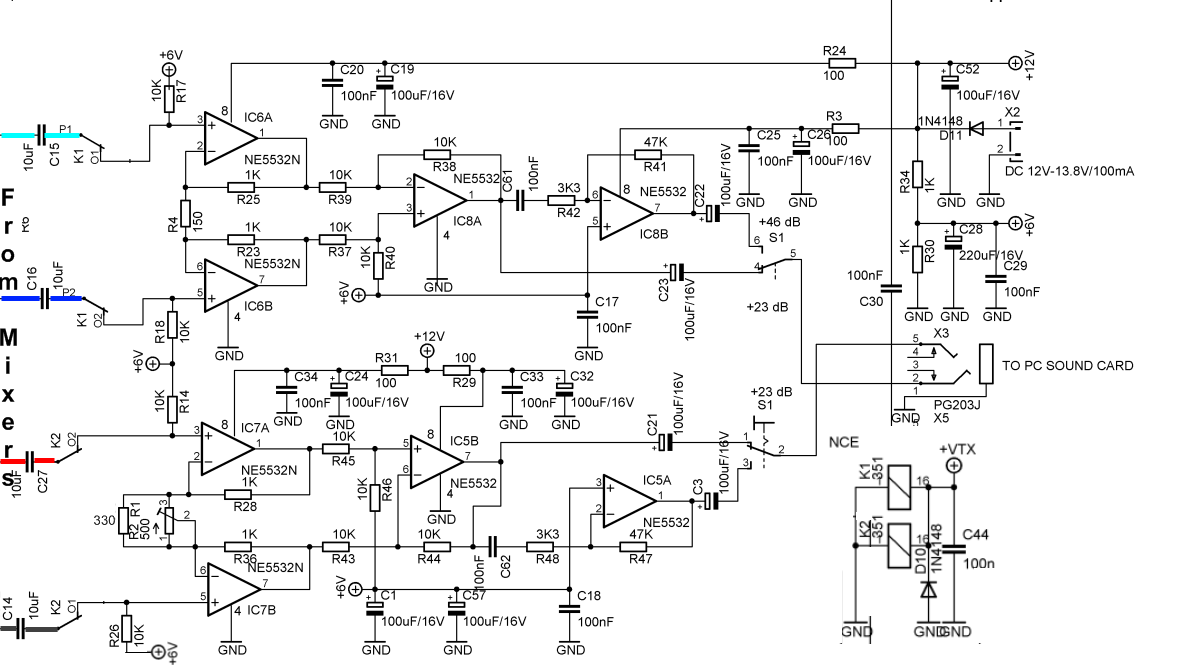
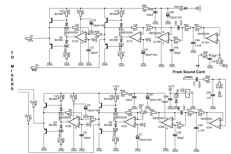
In this part of phase 3, the down-converted audio frequency signals (in quadrature) from the mixers are combined (0° + 180°, 90° + 270 °) and then summed and passed to the PC, either directly following the summing operatikon or passed through an amplification stage for a 23 db boost (as determined by S1), as I and Q outputs of the G40. The sub-schematic below shows the RX path for the opamps. (A similar path is defined for the TX opamps, where the I and Q signals from the PC are sent to the mixers and out to the RF line.)
RX OpAmps Schematic
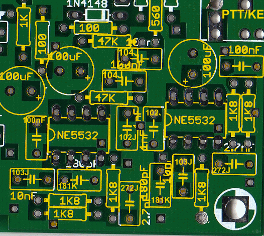
Following the schematic, below, are several graphics that split this sub-phase into graphics/parts, providing the location of components, by type.
BOM
| Capacitor 10 nF 103 MLC 50V | 2 |
| Capacitor 100 nF 104 MLC 50V | 15 |
| Capacitor 100nF 104J USM | 2 |
| Capacitor 10uF / 25V Non-polarized | 4 |
| Cap. Electrolytic 10uF 25V | 1 |
| Cap. Electrolytic 220uF 16V | 2 |
| Cap. Electrolytic 100uF 25V | 12 |
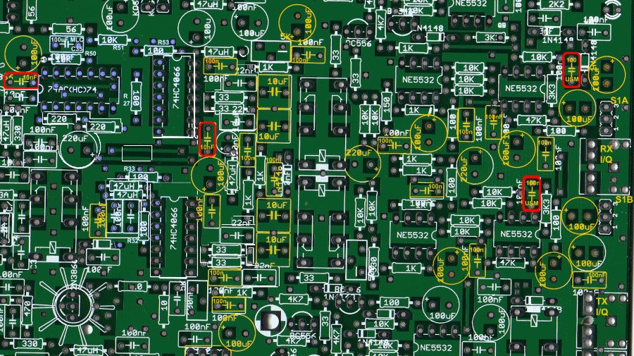
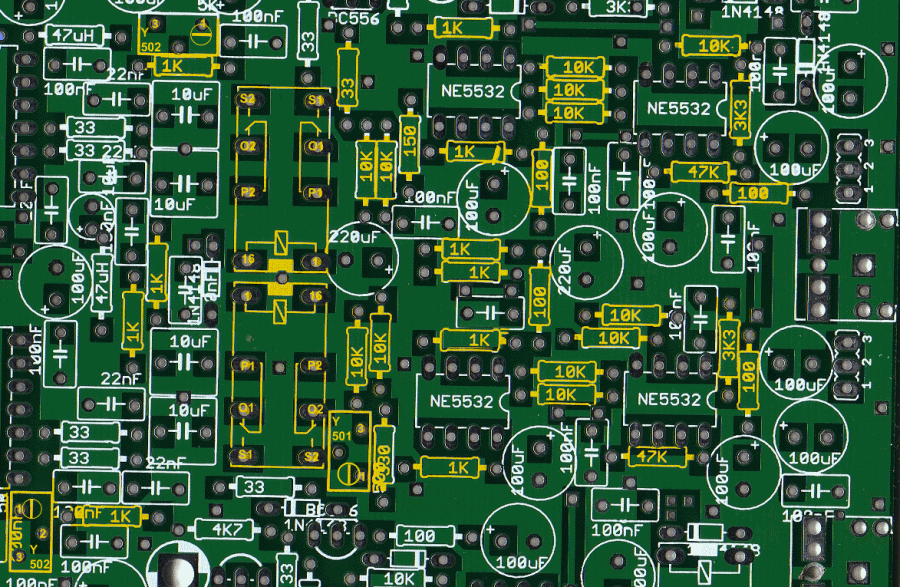
Capacitors Layout
A number of capacitors, electrolytc and non-electrolytic are installed for the RX Opamp, per the graphic below:
Resistors, etc. Layout
BOM
| Component | Qty |
|---|---|
| Resistor 10 K 1/4W | 12 |
| Resistor 100 Ohm 1/4W | 4 |
| Resistor 150 Ohm 1/4W | 1 |
| Resistor 1 K 1/4W | 10 |
| Resistor 33 Ohm 1/4W | 1 |
| Resistor 330 Ohm 1/4W | 1 |
| Resistor 3.3 K 1/4W | 2 |
| Resistor 47 K 1/4W | 2 |
| Trimmer pot. 500 Ohm Y501 | 1 |
| Trimmer pot. 5 K Y502 | 2 |
| Relay JRC27F/012 12V | 2 |
| Switch DPDT Mini | 1 |
| RCA stereo | 1 |
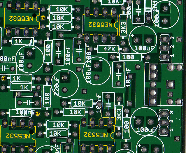
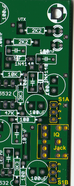
Similarly, a large number of resistors, along with three pots and 2 relays, are installed for the rx opamps, per the following diagram:
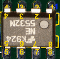
Operational Amplifiers - NE5532
BOM
| Component | Qty |
|---|---|
| IC NE5532P OpAmp | 4 |
The four NE5532s that provide the RX OpAmp chain are installed as the center two chains of an array of four chains of NE5532s. The builder needs to take care to install in the RX opamps' holes, not the TX opamps's holes. The builder must also pay close attention to the orientation of the opamps. They are installed such that their printing is upside down, with the marking dot oriented "top right".
Some have asked whether they could/should use sockets. The answer has been "It is OK to use sockets for these ICs, but the sockets must be of the highest quality" (a large cost issue). If the builder is NOT using sockets, follow the maxim "Measure twice, cut once", since these brutes are hard to get out once soldered in.
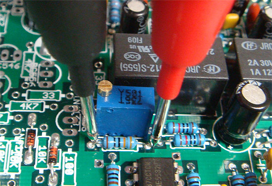
RX OpAmp Feedback Resistance Adjustment
With the power OFF, adjust trimpot Y501 until the resistance across the 300 ohm resistor is 150 ohms
Phase 3 Completion
BOM
| Component | Qty |
|---|---|
| BNC Connector 50 Ohm | 1 |
| RCA stereo | 1 |
| Hookup Wire | 15cm (6") |
Antenna Jack (BNC)
Mount the BNC Jack on the left-hand side of the board
RX I/Q Output Jack and Switch SW1
|
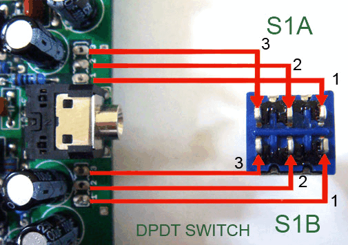
|
Temporary Connection Between Antenna and RX (Mixer Input)
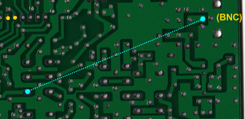
"Tack" solder a wire to connect the antenna "hot" pin on the BNC connector to the Mixer Stage's Input point on the board, as indicated below.
Phase 3 Testing
Phase 3 Current Consumption
Check RX current consumtion - it should ve very low, under 100m. Much higher current readng will indicate leakage to ground (possibly in phase 4) or very low current means no connection (blown diode).
Voltage Checks
6V Test
The testpoints shown below should test at 6V dc with respect to ground:
2.5V Test
The testpoints shown below should test at 2.5V dc with respect to ground:
NE5532 Pin Voltages
-check out voltages (with respect to ground) on each NE5532:
| Pins 1- 3 and 5- 7 | Pin 4 | Pin 8 |
|---|---|---|
| +6V dc | 0V dc | +12V dc |
NOTE: voltage measure on all four NE5532 should be identical.
If voltages are not as above
The exact voltage depends on out voltage of your power supply and with +12.5 V you should see the voltages specified above. Variation of +/- 1V is not critical.
According to a note in the reflector, it is OK to have 'wrong' voltages on NE5532 after the phase 3 and before wiring in the last phase. However once all wires are connected, the voltage reading on all NE5532 should be identical (http://groups.yahoo.com/group/GenesisRadio/message/88).
Comment from reflector: voltage on pin 8 depends on input (power supply) voltage. the higher the input, the higher the voltage on pin 8. But this is not critical on receive, any value around 11-12V is fine. Also even with voltage as low as 2.5V on all other pins of NE5532, receiver will still work ok (5-6V is recommended). However it is very important that all pins on all 4 NE5532 do have identical voltage
Additional Phase 3 Voltage Tests
Mixer ICs (each 74HC4066)
Pin 14 should read +5V dc. Pins 5, 6, 12, and 13 should each read 2.5V dc
Phase 3 - RX Testing/Adjustment
Connect an antenna to the BNC antenna jack on the G40
Connect the G40 to your PC using plug cables between the RX I/Q jack and the PC's Stereo Line-In input (or MIC input, if the PC has a stereo MIC input).
Fire up your SDR program of choice and set the center frequency at 7.047 MHz
Power on the G40. You should see some 40m signals if your RX is working. See the video of Bojan S51QA's test at this point.
Image Rejection Adjustment
It is crucial that after the build phase 3 image rejection is adjusted properly. As in all direct conversion receivers, the G40 starts up showing an image of the desired signal on the opposite side of the center frequency in the display. This is eliminated by properly adjusting the hardware, using the techniques described on the G40 website. Follow these techniques to correctly adjust your receiver.
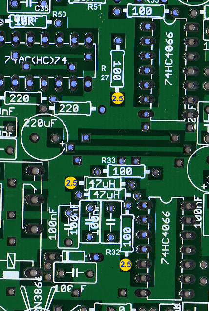
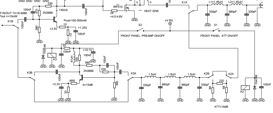
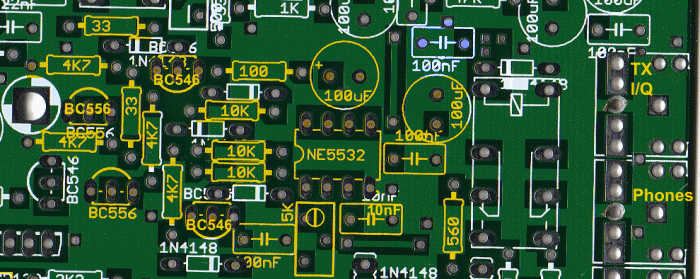
Phase 04: RX RF Filter, Attenuator and Antenna Switching
In phase 4, we put the finishing touches to the receiver, including some components that are shared by the transmitter. The circuit includes a switchable attenuator, a switchable RF pre-amp, and the relay-switched band-pass filters in the RF path to the antenna jack.
Remove Temporary Bottom Wire from Phase 3
Desolder and remove the length of wire connected between the Mixer stage's input and the BNC connector.
04a: Caps, Jumpers, Chokes, and Resistors
BOM
| Jumper wire (component leads) | 4 |
| Capacitor 100 nF 104 MLC 50V | 9 |
| Capacitor 330 pF [331] NPO 100V | 4 |
| Capacitor 680 pF [681] NPO 100V | 3 |
| Resistor 1.5 K 1/4W | 1 |
| Resistor 220 Ohm | 2 |
| Resistor 33 Ohm 1/4W | 2 |
| Resistor 330 Ohm 1/4W | 1 |
| Resistor 390 Ohm 1/4W | 1 |
| Resistor 560 Ohm 1/4W | 1 |
| Resistor 6.8 Ohm 1/4W | 1 |
| Resistor 68 Ohm 1/4W | 2 |
| Choke 1.5 uH | 2 |
| Choke 1.8 uH | 1 |
| Choke 47uH | 1 |
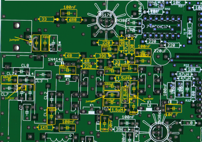
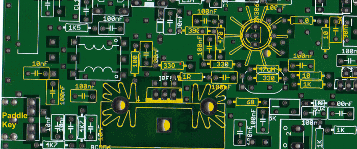
PCB Layout
The first portion of phase 4 installs 4 jumper wires along with the resistors, capacitors, and chokes. The online assembly pictorial has an error: one 100uF capacitor was missing from the picture. The graphic below depicts the correct placement and identification of the components in this part of the Bill of Materials
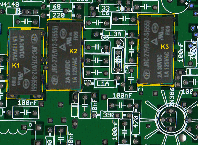
04b: Relays
Install the three relays, K1-K3. Note the orientation of K1 vs. the orientation of K2 and K3.
BOM
| Component | Qty |
|---|---|
| Relay JRC27F/012 | 3 |
PCB Layout
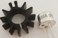
04c: Install PreAmp Transistor 2N3866 With Heat Sink
BOM
| Component | Qty |
|---|---|
| Heat sink TO-39 | 1 |
| Transistor 2N3866 | 1 |
Prepare Transistor and Heat Sink
|
NOTE: the heat sink is factory supplied so tight that it would not be possible to place it over the 2N3866 after the transistor is soldered to the PCB. Therefore it is important to insert the 2N3866 into the heat sink first. |
|
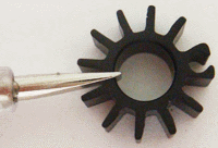
Prepare the heat sink by gently spreading its collar. |
|
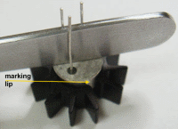
Place the transistor over the heat sink with the marking lip in the middle of the gap, push it down with the flat side of metal tweezers. The grip should be firm and tight (if it is too tight or loose, remove the transistor and adjust the collar) |
|
|
The transistor and its heatsink will resemble this when ready for mounting |
|
|
Place the 2N3866 into PCB (marking lip alignment as per photo). Solder it approx 4-5 mm (about 3/16") above PCB, just enough to clear any surrounding components. TIP: Initially, solder one lead only. Then adjust for height and level, as needed, and then solder the other two leads. |
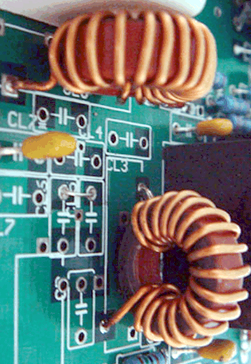
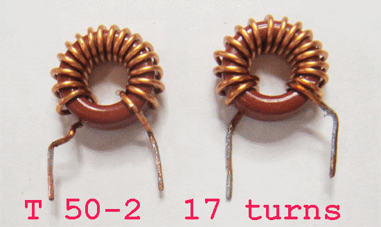
04d: Wind and Install Toroidal Inductors - L1 and L2
BOM
| Component | Qty |
|---|---|
| Torioid core T50-6 | 2 |
| Wire, Magnetic | ~1m (35") |
Wind/Install
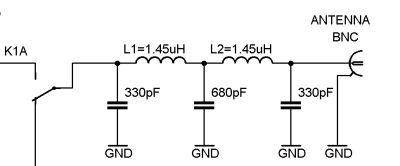
This transceiver requires exactly two wound toroids! L1 and L2 (each 1.45 uH) are each wound on a T50-2 core with 17 turns of 0.8 mm (#20 AWG) wire, exactly as per photo. Make sure to remove enamel coating and tin the leads before mounting. The length of wire required for each coil is about 13-14" (about 35 cm).
Inductors Continuity Test
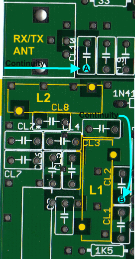
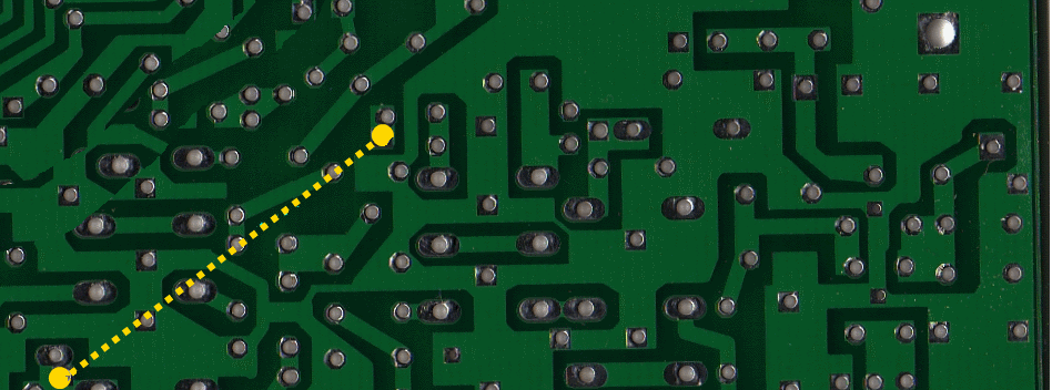
You can test the installation of the inductors with the power OFF by measuring the resistance between two test points: the jumper wire at point "A" and the empty capacitor hole at point "B" (see PCB layout above, points designated "A" and "B") that are connected via board traces to the soldered-in inductors. If you get zero resistance between the points, you can trust you have tinned and soldered them correctly.
Install Underside Wire
Install a length of wire on the borrom of the board between the 33 ohm resistor and the K3 relay
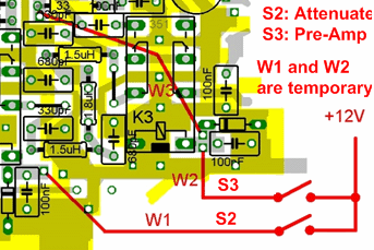
Temporarily Install the Attenuator and Pre-Amp Switches (SW2 and SW3)
Depending upon the kitting, these switches will either be SPST or DPDT, acting as SPST switches. They are temprorarily wired into the board so we can test the RX and the attenuation and preamplification circuits.
Run a temporary connection between each switch and the 12-13.8 V dc rail (this connection will later be exchanged for a connection to VRX, once it is enabled).
BOM
| Component | Qty |
|---|---|
| Switch SPDT Mini | 2 |
Tests (Power = ON)
Test Attenuator and Pre-Amp Operation
Attenuator
To test attenuator preamplifier: tune the SDR PC program to 40m signal (or connect signal generator) with S2 (attenuator) switch on, receiving signal will decrease for approximately 17dB.
PreAmplifier
After the attenuator test, turn off the attenuator and turn on the RF preamplifier (S3, pre-amp switch) and you will notice signal strength improvement of 15dB.
Voltage Test
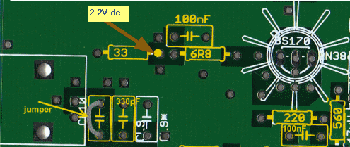
Measure the voltage at the testpoint shown below - should read 2.2V dc (with respect to ground). The testpoint is the "north" end of the wire that was installed to the underside of the board.
RX Construction Complete
With these tests, the receiver is completely adjusted. Now, on to the transmitter!
Phase5 - CW Monitor
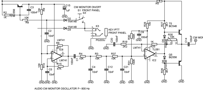
Schematic
Note: Not all components in the Bills of Material below are represented on this schematic. It is provided for reference only.
Install 19 Resistors
Layout
BOM
| Component | Qty |
|---|---|
| Resistor 1 Ohm 1/4W | 1 |
| Resistor 1 K 1/4W | 2 |
| Resistor 10 K 1/4W | 6 |
| Resistor 100 K 1/4W | 2 |
| Resistor 100 Ohm 1/4W | 1 |
| Resistor 2.2 K 1/4W | 1 |
| Resistor 330 Ohm 1/4W | 2 |
| Resistor 4.7 K 1/4W | 3 |
| Resistor 47 K 1/4W | 1 |
Install 16 Capacitors
Layout
BOM
| Component | Qty |
|---|---|
| Cap. Electrolytic 1 uF 25V | 1 |
| Cap. Electrolytic 100uF 25V | 1 |
| Capacitor 10 nF 103 MLC 50V | 5 |
| Capacitor 100 nF 104 MLC 50V | 9 |
Remainder
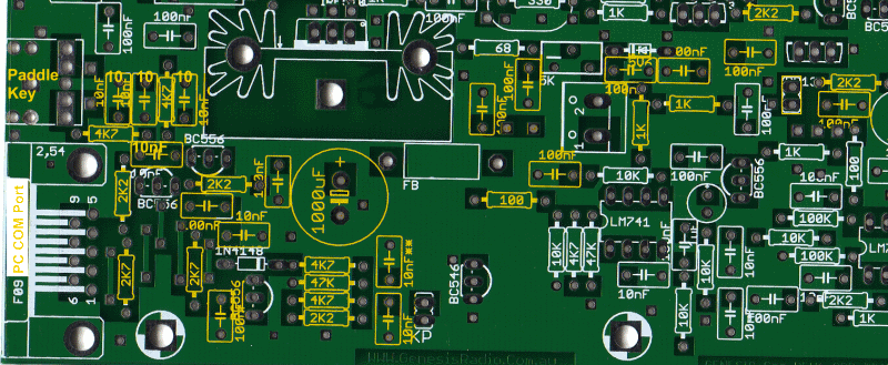
Solder the remaining components for Phase 5. Pay attention to the locations of BC556 and BC546 transistors and the alignment/orientation of the OpAmps IC uA741!
Layout
BOM
| Component | Qty |
|---|---|
| RCA stereo Connector | 3 |
| Relay JRC27F/012 12V | 1 |
| Trimmer pot. 10 K Y103 | 1 |
| IC uA741 | 2 |
| Transistor BC546 C546 | 1 |
| Transistor BC556 C556 | 2 |
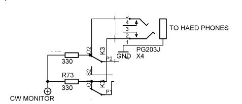
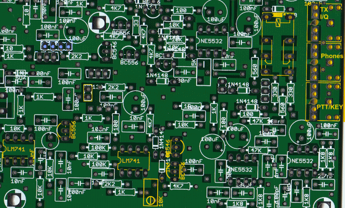
Wires and Switches
Install Three Temporary Wires
Install the three temporary wires, presented ad dotted lines in the graphic below. These can be installed on either the topside or the underside of the board, according to the builder's preference.
- 12-13.8v dc power lines (remove previous power leads from top right corner)
- connector wire to patch CW Monitor audio to
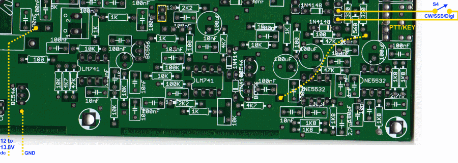
Install S4 - CW/SSB/Digimode Switch
Using an SPST (or DPDT acting as SPST) switch, connect the switch and wires as shown in the graphic below. (S4 is represented variously on in the G40 docs as S3; switch designations were reworked to adjust for the duplication of S1 in earlier phases)
Layout
BOM
| Component | Qty |
|---|---|
| Switch DPDT Mini | 1 |
| Hookup wire | n/a |
Testing Phase 5 CW Monitor
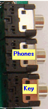
Plug in phones, key and connect power supply via newly added wires.
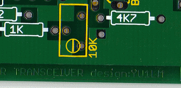
Adjust CW sidetone volume with trimmer Y103 (10K).
Phase 6 - PC RX/TX Control
Schematic
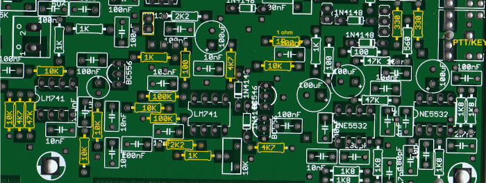
Install Capacitors and Resistors
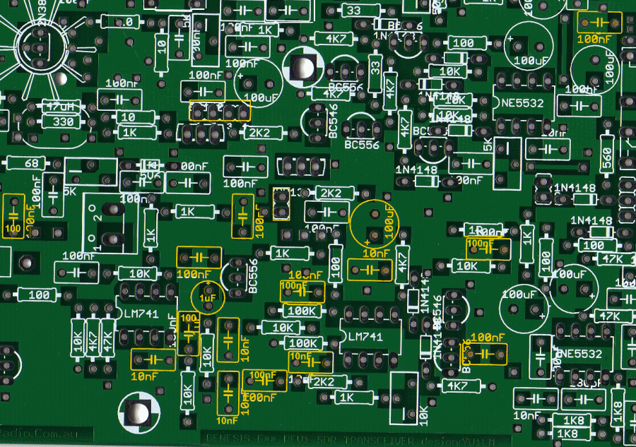
Be careful - there are some easily confused values in the resistors (2.2 vs 2.7 k; 4.7k vs 47k, etc.). Note Also the locations of the seven 10nF capacitors vs. the ten 100 nF capacitors
BOM
| Component | Qty |
|---|---|
| Cap. Electrolytic 1000uF 25V | 1 |
| Capacitor 10 nF 103 MLC 50V | 7 |
| Capacitor 100 nF 104 MLC 50V | 10 |
| Resistor 1 K 1/4W | 2 |
| Resistor 100 Ohm 1/4W | 1 |
| Resistor 2.2 K | 5 |
| Resistor 2.7 K | 2 |
| Resistor 4.7 K 1/4W | 4 |
| Resistor 47 K 1/4W | 1 |
Install BD139 and BD140 Transistors
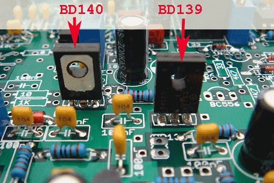
BOM
| Transistor BD139 | 1 |
| Transistor BD140 | 1 |
Install the Remainder of the Parts
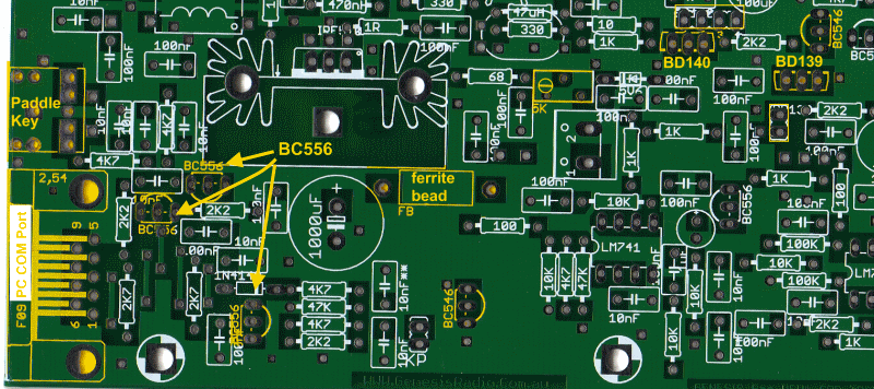
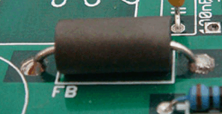
Ferrite Bead
BOM
| Component | Qty |
|---|---|
| Ferrite bead FS2-43 | 1 |
| DB9 9-pin female | 1 |
| RCA stereo Connector | 1 |
| Trimmer pot. 5 K Y502 | 1 |
| Transistor BC546 C546 | 2 |
| Transistor BC556 C556 | 3 |
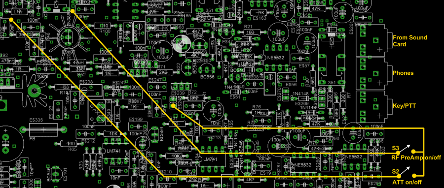
Install Permanent Jump Wires and Vin Wires
S2 and S3 from Phase 4
Rewire switches S2 and S3 (from Phase 4) by removing their temporary wiring and installing permanent wiring as below:
Install Permanant Vin Wiring
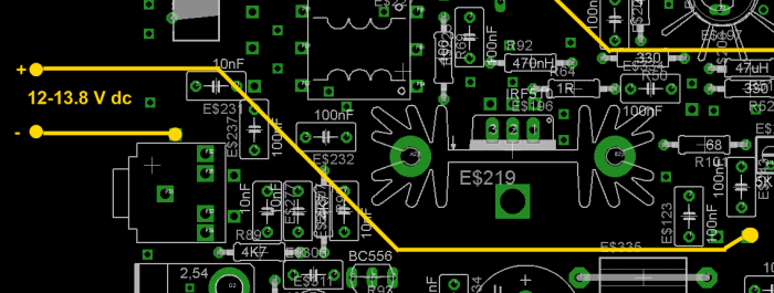
Disconnect +Vin temporary lines from lower left corner area of the pcb
Install permanent +Vin
Install Jump Wire
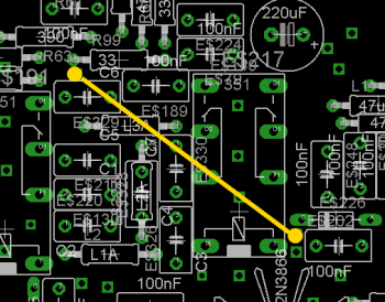
Connect Remaining Jump Wires
Topside
Underside
PC RX/TX Control Testing
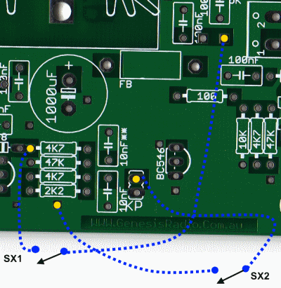
Connect Temporary Switches/Wires SX1 and SX2
In order to test the PC PX/TX Control, we need to temporarily hook up a couple of switches, per the diagram below:
Tests
PC RX/TX control testing should be performed in 2 steps:
- Step1:
- Using a DMM, measure the voltage at +VTX. It should be 0V and voltage at +VRX=+12-+13.8V.
- Set switch SX1 ON. When switch SX1 is ON, +VTX will measure +12-13.8V and +VRXwill be 0V.
- Step 2:
- Turn SX1 OFF.
- Connect Genesis G40 to the serial PC port directly or via USB/ Serial adapter.
- Settings in SDR software should be set according to the table 1 (see above).
- Turn on SX2 and +VTX should be +12-+13.8V.
Phase 7 - TX Sample and Hold Modulator
This phase takes two signals (I and Q) from the PC Soundcard and produces four quadrature outputs to the bilateral mixing switches. The process is essentially the reverse of the RX side. Since the mixers are bilateral, the TX signals in quadrature go through the same process of sampling and holding, clocked by the Quadrature signals from the dividers.
Schematic
Reinstall CW Monitor Temporary Wire (from Phase 5)
Find the temporary wire placed during Phase 5 to enable CW Monitoring; reinstall the wire on the underside of the board.
Install Bottom Right Components
Install components in the order listed below:
BOM
| Component | Qty |
|---|---|
| RESISTORS | |
| Resistor 1 K 1/4W | 1 |
| Resistor 1.8 K 1/4W | 6 |
| Resistor 100 Ohm 1/4W | 2 |
| Resistor 47 K 1/4W | 2 |
| Resistor 560 Ohm 1/4W | 1 |
| MLC CAPACITORS | |
| Capacitor 100 nF 104 MLC 50V | 2 |
| ICs | |
| IC NE5532P | 2 |
| USM CAPACITORS | |
| Capacitor 1 nF [102J] USM | 2 |
| Capacitor 10 nF [103J] USM | 2 |
| Capacitor 100 nF 104J USM | 2 |
| Capacitor 180 pF [181J] USM | 2 |
| Capacitor 2.7 nF [272J] USM | 2 |
| ELECTROLYTIC CAPACITORS | |
| Cap. Electrolytic 100uF 25V | 3 |
Upper Right Components
Install components in the order listed below:
BOM
| Component | Qty |
|---|---|
| Resistor 3.3 K 1/4W | 1 |
| Resistor 33 Ohm 1/4W | 1 |
| Resistor 4.7 K 1/4W | 4 |
| Resistor 10 K 1/4W | 3 |
| Resistor 100 Ohm 1/4W | 1 |
| Capacitor 100 nF 104 MLC 50V | 1 |
| Transistor BC546 C546 | 2 |
| Transistor BC556 C556 | 2 |
| IC NE5532P | 1 |
| Cap. Electrolytic 100uF 25V | 2 |
Mid-Right Components
Install components in the order listed below:
BOM
| Component | Qty |
|---|---|
| Resistor 10 K 1/4W | 3 |
| Resistor 100 Ohm 1/4W | 1 |
| Resistor 33 Ohm 1/4W | 2 |
| Resistor 4.7 K 1/4W | 4 |
| Resistor 560 Ohm 1/4W | 1 |
| Capacitor 10 nF 103 MLC 50V | 1 |
| Capacitor 100 nF 104 MLC 50V | 2 |
| Transistor BC546 C546 | 2 |
| Transistor BC556 C556 | 2 |
| IC NE5532P | 1 |
| Cap. Electrolytic 100uF 25V | 2 |
| Trimmer pot. 5 K Y502 | 1 |
Before you can check voltage on NE5532's in phase 7, ensure you connected the permanent wires specified at the end of Phase 6. Those wires supply + voltage to the four TX NE5532 installed above. Basically make sure that you have +12 to 13V on pin 8 on all NE5532.
Adjust Trimmer
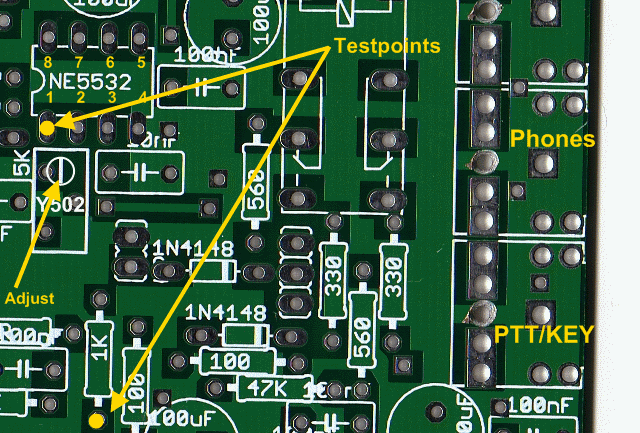
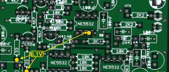
Connect your ohmmeter between the following points : pin 2 of the NE5532 and the 1K resistor.
Adjust the trimmer Y502 until the ohmmeter reads 3.3KΩ
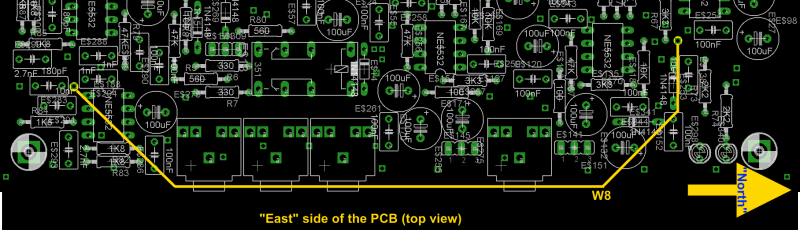
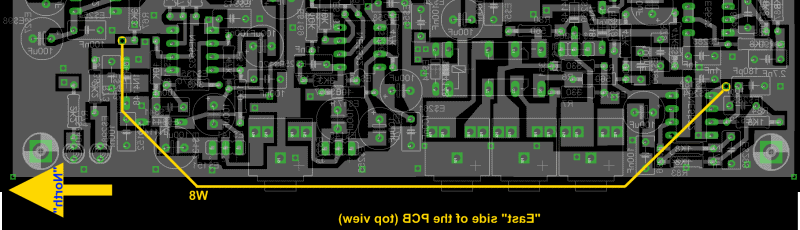
Install Permanent Wires
Install "W8" to topside or inderside of the board, as fits your preference. Images below represent the topside and underside views of the placement of W8. (Note: the graphics are turned on their side to accomodate the length of the wire.)
Phase 7 Testing
From Assembly Pictorial for Phase 7
Apply power to the board.
Check out voltage on all 8 ICs NE5532:
pins 1,2,3,5,6,7. [+5.70V to + 6.00V]
This voltage must be identical on all of the specified pins for all eight ICs.
Note that the RX ICs are installed with their "1" pins at the upper right of each chip; the TX ICs are installed with the "1" pin at the lower left of each IC.
From Manual, Phase 7
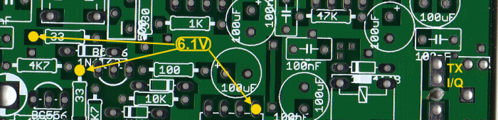
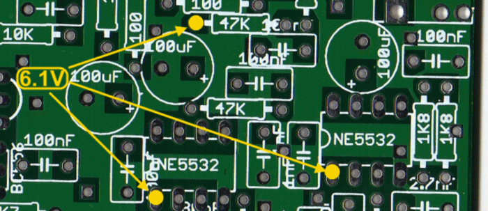
Testpoints - PCB Upper Right
Testpoints - PCB Middle Right
Testpoints - PCB Lower Right
Phase 8 - RF FET Power Amplifier and Driver
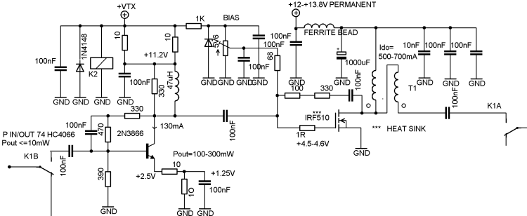
The upconverted RF (from the modulated AF I and Q signals' processing in the Store and Hold Mixer) is passed via the mixer's input/output line to the driver 2N2866 and, thence, to the IRF510 FET PA, and on through the low pass filters, to the antenna.
.Schematic
Install All Components, Except FET and Transformer
BOM
| Component | Qty |
|---|---|
| Capacitor 10 nF 103 MLC 50V | 1 |
| Capacitor 100 nF 104 MLC 50V | 8 |
| Choke 47uH | 1 |
| Resistor 1 Ohm 1/4W | 1 |
| Resistor 1 K 1/4W | 1 |
| Resistor 10 Ohm 1/4W | 3 |
| Resistor 100 Ohm 1/4W | 1 |
| Resistor 330 Ohm 1/4W | 3 |
| Resistor 390 Ohm 1/4W | 1 |
| Resistor 470 Ohm 1/4W | 1 |
| Resistor 68 Ohm 1/4W | 1 |
| Heat sink TO-39 | 1 |
| Transistor 2N3866 | 1 |
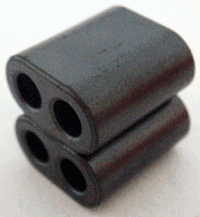
Wind and Install the Dual Binocular Transformer
BOM
| Component | Qty |
|---|---|
| BN43-202 Core | 2 |
| Wire Cul | - |
(see the assembly pictorialon the GenesisRadio website.)
Cores
Glue together the two binary cores as indicated in the graphic, below:
Twisted Wire
Prepare a 40 cm (~16") long piece of enameled copper wire and fold it over so that it is two 20 cm wires joined at the one end
twist the wires together so that you get approximately three twists per 10 cm (~4") of length
Wind the Wire through the Core
Thread the twisted wires (folded end first) through the glued cores, starting in hole 1, coming out the other end and looping back through the top core to exit at hole 3. Continue from hole 3 into hole 2, coming out the other end and looping back into the upper core so as to exit at hole 4. .
When finished winding, cut the folded end of the twisted wire off, such that you noe have four wire ends.
The pair at hole 1 represents the primary leads; the pair at hole 4 represents the secondary leads of the wound transformer.
Using an ohm meter, identify the ends of each wire as indicated on the graphic above. You may want to use a small piece of colored hookup wire insulation to identify the "a" (or, if you prefer, the "b") wire's ends.
Mount the Transformer
You do not need to worry how to figure out the phasing; if you match the designated leads (a1, b1, a, b) with the holes as marked in the graphic below, you will have correct phasing.
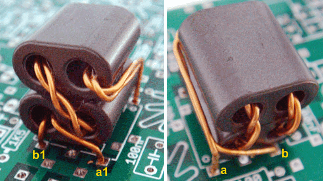
Insert transformer's leads into the PCB holes, as indicated above. Form the leads and pull them tight. Then cut off the excess (on the underside of the board) so that approximately 5mm (1/8") of wire is protruding out on the underside of the board.
Remove the transformer from the PCB, scrape the enamel coating from the 4 leads but DO NOT TIN them as yet (tinning the leads could cause them to be too "fat" to go back into the holes).
Insert the 4 transformer leads back into the PCB and solder them.
Install FET and Heat Sink
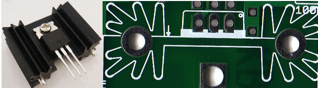
Attach the IRF510 power MOSFET to its heat sink with the M3 screw and nut.
Then solder the IRF510 leads and the two heat sink pins, such that the Transistor side of the heat sink is facing "north" and the blank side of the heat sink is facing "south".
BOM
| Component | Qty |
|---|---|
| Screw and nut M3 | 1 |
| Heat sink TO-220 | 1 |
| Transistor IRF 510 | 1 |
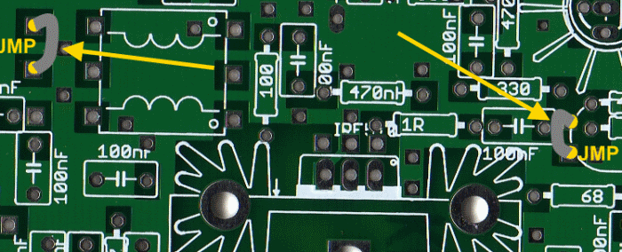
Install two Jump Wires
Using two pieces of cut-off component lead wires, solder jumper wires as indicated below
WIP BOM
Work-in-Progress - Phase BOM
BOM
| Component | Qty |
|---|
To be continued
->