Introduction
Theory of Operation
The local oscillator (U4) is a programmable oscillator, whose programmatic parameters are set by the USB interface, U2.
The user, operating special SDR software on the PC, selects a desired center frequency. The PC issues commands, via a USB port, to U2 (the USB control chip from the preceding stage. These commands will result in U4's producing a frequency that is exactly 4 times the desired center frequency selected in the SDR program.
U2 responds to commands from the PC, translating them into commands in the I2C protocol to control the programmable oscillator U4. (If the I2C commands are not received by U4, it would default to an output frequency of 56.320 mHz.)
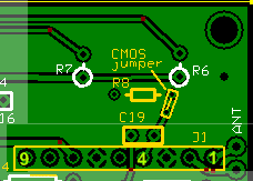
The IC U5 is needed if the version of U4 is the "LVDS" version. If U4 is a CMOS version, U5 (and R8) are not required and, instead, a jumper wire is installed to bypass them.
This LO stage must produce an output rf signal (available at J1 pin 4) that is four times the desired center frequency for the radio. This is then fed to the dividers/phasors section to produce the two center-frequency signals that are in quadrature and ¼ the LO frequency.
Schematic
This is a subset of the overall schematic. Note: red dot indicates resistor testpoints (hairpin, top, or left-hand lead)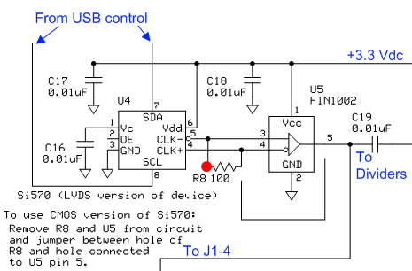
Bill of Materials
Note:
Occasionally, Tony is required by logistical issues beyond his concern to ship the Si570 chip in a separate, later shipment. This is due to lead time considerations on his bulk orders from SiLabs, making it impossible to ship the complete kit in one shipment.
| Designation | Value | Color/Code | Orientation | Category | Notes |
|---|---|---|---|---|---|
| U5 | FIN1002 | FN02X |
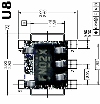 | SMT | only required for LVDS version of Si570 |
| U4 | Si570 (CMOS version of device) |
 | SMT | (see note above concerning partial shipments) | |
| C16 | 0.01uF | SMT 1206 | |||
| C17 | 0.01uF | SMT 1206 | |||
| C18 | 0.01uF | SMT 1206 | |||
| R08 | 100 |  | flat-h | omit for CMOS | |
| J1 | 9 pin | ||||
| C19 | 0.01uF | 103 | ceramic |
Summary Build Notes
- Install U5 - only for LVDS version of Si570 (bottom)
- Install U4 (bottom)
- Install 3 SMT capacitors (bottom)
- Install resistor (top, if LVDS)
- Install main bus jack, J1
- Install ceramic cap C19
- Install CMOS jumper wire (if Si570 is CMOS versio)
- Test the Stage
Detailed Build Notes
Bottom of the Board
Install U5
| Designation | Value | Color/Code | Orientation | Category | Notes |
|---|---|---|---|---|---|
| U5 | FIN1002 | FN02X |
|
SMT SOT-23 | LVDS only: do not install if U4 is a CMOS version. |
Install U4
Orientation: Check the Bottomside view, below, to see the proper orientation for U4's installation.
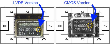
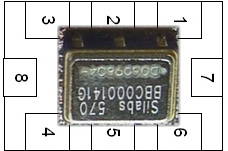
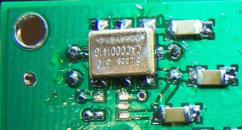
Note: There are two versions of the Si570, the CMOS and the LVDS. See the chart below for how to distincuish them (the chips are shown in their mounting orientation for this kit). See Softrock Group message for discussion of differences.
| Designation | Value | Color/Code | Orientation | Category | Notes |
|---|---|---|---|---|---|
| U4 | Si570 |
|
SMT | (LVDS version shown) |
Install SMT Capacitors
| Designation | Value | Color/Code | Orientation | Category | Notes |
|---|---|---|---|---|---|
| C16 | 0.01uF | SMT 1206 | |||
| C17 | 0.01uF | SMT 1206 | |||
| C18 | 0.01uF | SMT 1206 |
Top of the Board
Install Resistor (see notes)
| Designation | Value | Color/Code | Orientation | Category | Notes |
|---|---|---|---|---|---|
| R08 | 100 | | flat-h | omit for CMOS |
Install Ceramic Capacitor C19
| Designation | Value | Color/Code | Orientation | Category | Notes |
|---|---|---|---|---|---|
| C19 | 0.01uF | 103 | ceramic |
Install CMOS Jumper (only required of Si570 is CMOS version
| Designation | Value | Color/Code | Orientation | Category | Notes | |
|---|---|---|---|---|---|---|
| short jumper wire |
Install Main bus Jack J1
Note: J1 through J3 all mount on top of the circuit board with the short pins through the board for soldering the connector in place| Designation | Value | Color/Code | Orientation | Category | Notes |
|---|---|---|---|---|---|
| J1 | 9 pin |
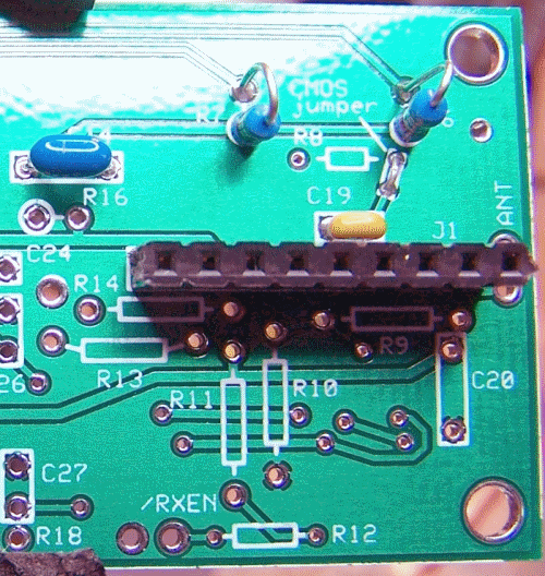
Completed Stage
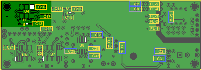
Topside
Bottomside
Testing
Current Limited Power Test
- Connect a 1 k ohm resistor in series with the power line and apply 12 V dc power
- the current should be relatively low (around 10 mA or less). Author's results = 8.1 mA
- Measure the voltage WRT ground at the +5 V testpoint at J2.
- A voltage of around 1-2 V dc indicates the power rail is not shorted. Author's results = 997 mV
Current Draw (DMM)
- Current draw here is for the CMOS version of the Si570. Adjust these numbers up by about 14 - 20 mA for the LVDS version.
- With the USB cable unplugged, power up the board, and measure the current draw. This should now go to around 70-80 mA. Author's results 75.4 mA
SI570 Control/Configuration Test
In the preceding stage, you had downloaded and installed Fred PE0FKO's CFGR.exe and SRDDLL.dll files.
Power up your V9.0 board and plug in the USB cable to the PC and the V9.0 board.
Run the CFGR.exe program, again, referring to the instructions on Fred's site, and go to the USB tab. In the USB tab, verify that your PC is "seeing" the Microcontroller on the V9.0 board.
Then, go to the "SI570" Tab and make sure the settings are as indicated in the graphic below:

(This sets the LO to oscillate at 28.2MHZ, a frequency which will yield a center frequency, via the dividers, of 7.05MHz)
Click on the "Reboot" button. This will reboot the firmware. A USB disconnect will happen, and with auto connect, it will connect again and the SI570 should startup at 28.2 MHZ.
Verify LO Output
- fashion a small wireloop "antenna" to plug into Pin 4 of J1
- connect a wire to your transceiver's RX ANT jack and loop it through the "antenna" in pin 4 of J1
- Tune the transceiver to receive at 28.200 MHz (4x 7.05 MHz)
Now, try the same exercize but using 14.1MHz (for a center frequency of 3.525MHz). Just go to the "Tune" tab in CFGSR (The 'Tune' tab in CFGSR is in effect a stand alone VFO controller, so whatever frequency you set it to, the Si570 will generate an output at four times that. That is the easiest way to change the LO output frequency.) Then, measure the frequency of the SI570 LO.
LO Output (Scope/Freq Counter)
The Local Oscillator should output a signal at the four times the center frequency selected by Rocky.
Do not attempt this measurement unless you have a calibrated scope of very good quality and correctly compensated probes.
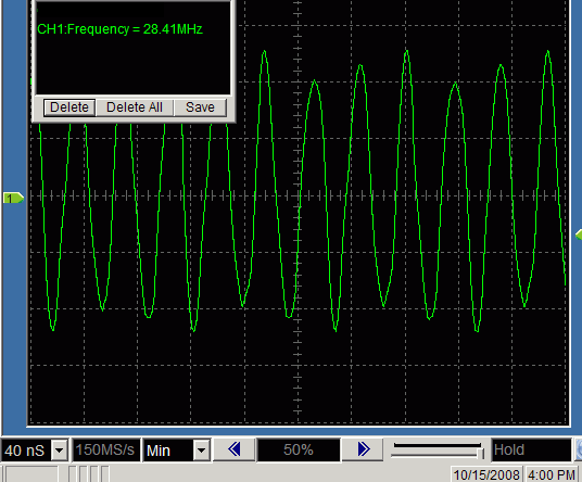
Test
-

- Tune the USB oscillator settings to get a center frequency of 7.046 MHz
- Apply power to the board
- Test the output of (U8 in the LVDS version of the kit or U4 in the CMOS version)
at pin 4 of J1: the frequency should be 28.184
MHz (4 times the desired center frequency of 7.046 MHz).
The AC pk-pk voltage should be aproximately or less than 3.3 V p-p.
The waveform should approximate be a square wave. - If you get 56.32 MHz (or 14.08 times 4) with tuning set as above, or regardless
of the frequency selected, this means:
- U2 has been incorrectly installed or
- pins 7 or 8 of U4 may have bad solder joints
- The USB interface is not working to receive the control signals from the software
- The software is not configured correctly to use the USB interface
LO Output Test for 40m (frequency measurement is approximate, at best)