RX Mixers/OpAmps Introduction
General
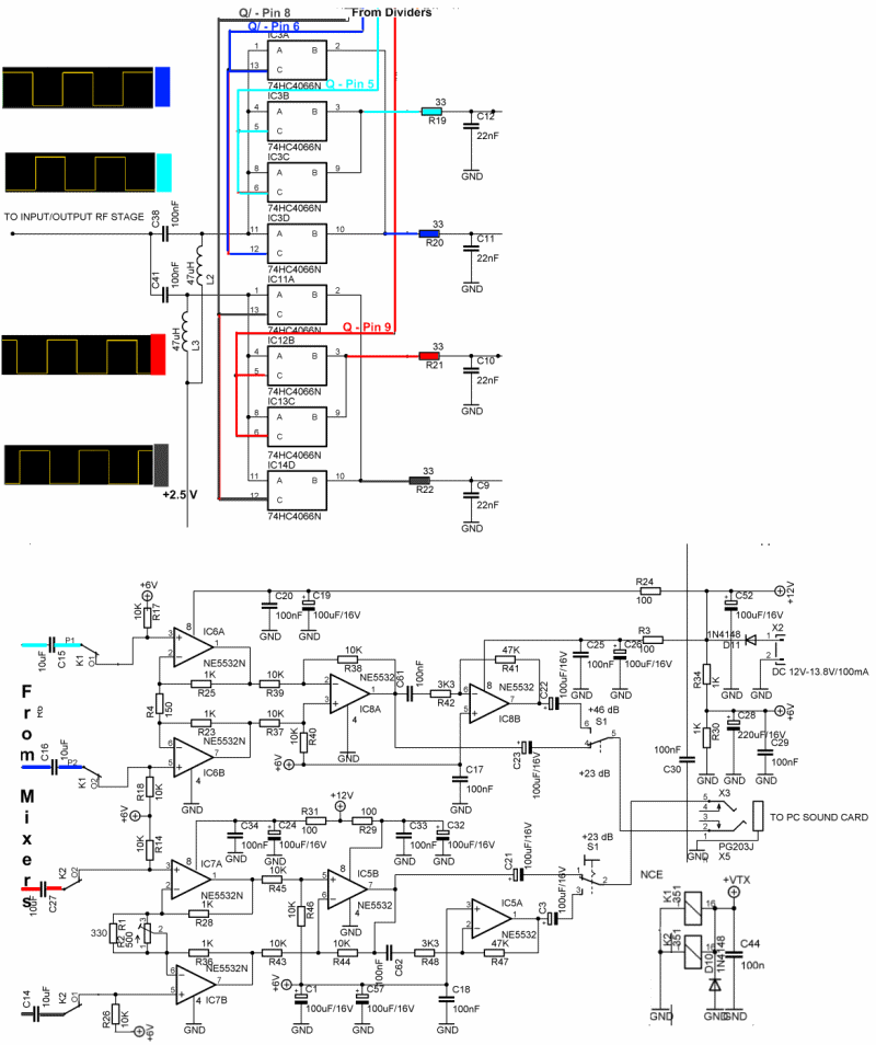
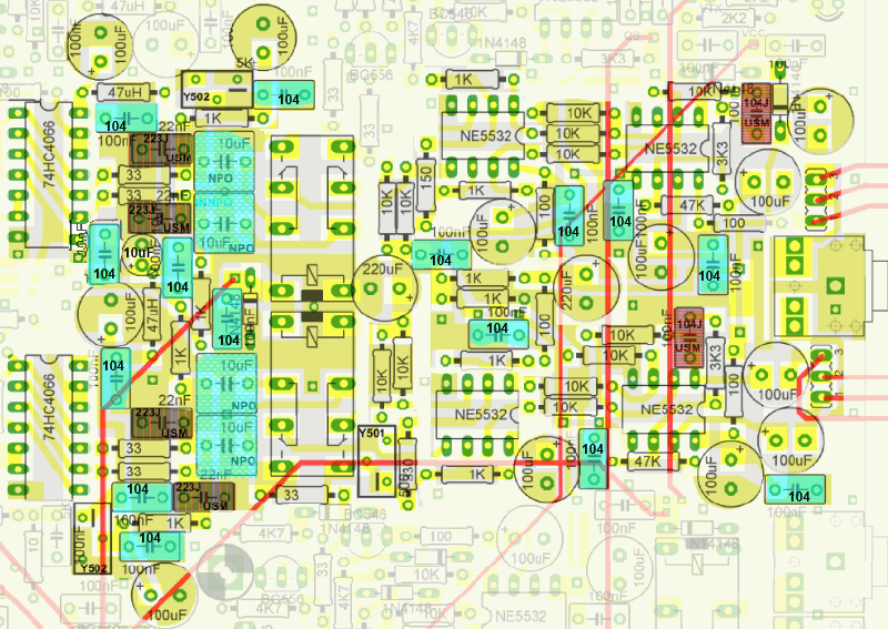
The G3020's mixer is a double-balanced, sample and hold circuit using two quad bilateral analog switches (74HC4066), clocked by the four outputs from the dividers.
Each pair of switches outputs to an RC pair that samples and holds the output for forwarding to the OpAmps Section. The portion of the schematic illustrating this is shown below (including divider output waveforms derived from a simulation of the divider operation). Not shown is that part of the circuit that uses two 5k trimpots for hardware balancing of the mixer.
The incoming RF is split into 2 streams, each going to two pairs of switches. Each switch pair is turned on and off by a signal coming from the dividers. The switched outputs of the pair are integrated by the corresponding RC circuit. As in the Tayloe detector, the result is the down-conversion of the RF signals to their AF analogues.
In the OpAmps sub-stage, the down-converted audio frequency signals (in quadrature) from the mixers are combined (0° + 180°, 90° + 270 °) and then summed and passed to the PC, either directly following the summing operation or passed through an amplification stage for a 23 db boost (as determined by S1), as I and Q outputs of the G3020.
The sub-schematic below shows the RX path for the opamps. (A similar path is defined for the TX opamps, where the I and Q signals from the PC are sent to the mixers and out to the RF line.)
(go directly to build notes)RX Mixers/OpAmps Schematic
(go directly to build notes)
RX Mixers/OpAmps Bill of Materials
Stage Bill of Materials
(resistor images and color codes courtesy of WIlfried, DL5SWB's R-Color Code program)
| Check | Count | Component | Marking | Category |
|---|---|---|---|---|
| ❏ | 10 | 1 k 1/4W 1% | br-blk-blk-br-br
 | 1/4W |
| ❏ | 4 | 100 1/4W 1% | br-blk-blk-blk-br
 | 1/4W |
| ❏ | 12 | 10K 1/4W 1% | brn-blk-blk-red-brn
 | 1/4W |
| ❏ | 1 | 150 1/4W 1% | brn-grn-blk-blk-brn
 | 1/4W |
| ❏ | 5 | 33 1/4W 1% | ora-ora-blk-gld-brn
 | 1/4W |
| ❏ | 1 | 330 1/4W 1% | ora-ora-blk-blk-brn
 | 1/4W |
| ❏ | 2 | 3k3 1/4W 1% (3.3K) | ora-ora-blk-brn-brn
 | 1/4W |
| ❏ | 2 | 47K 1/4W 1% | yel-vio-blk-red-brn
 | 1/4W |
| ❏ | 2 | JRC27F/012 relay | JRC27F/012
 | 12V relay |
| ❏ | 2 | 1N4148 | 1N4148
 | Axial |
| ❏ | 1 | 10 nF (.01uF) | 103
 | Ceramic |
| ❏ | 14 | 100 nF | 104
 | Ceramic |
| ❏ | 2 | 47 uH molded inductor 10% | yel-vio-blk-slv
 | Choke |
| ❏ | 1 | shunt wire (cut-off lead) | Cutoff | |
| ❏ | 2 | 74HC4066 Quad Bilateral SW |
 | DIP-14 |
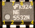
| ❏ | 4 | NE5532 Dual OpAmp | NE5532
 | DIP-8 |
| ❏ | 1 | 10 uF/25Vdc |
 | Electrolytic |
| ❏ | 12 | 100 uF/25Vdc |
 | Electrolytic |
| ❏ | 2 | 220 uF/25Vdc |
 | Electrolytic |
| ❏ | 1 | misc hookup wire | Hookup | |
| ❏ | 1 | BNC Connector Male - PCB mount |
 | Jack |
| ❏ | 1 | 3.5mm stereo jack - PCB mount (rt-angle) |
 | Jack-RA |
| ❏ | 2 | 100 nF USM | 104J
 | Metalized polyfilm |
| ❏ | 4 | 22 nF USM | F98 223J or F87 223J
 | Metalized polyfilm |
| ❏ | 4 | 10 uF (NP) |
 | Non-Polarized |
| ❏ | 1 | 500 (Y501) | Y501
 | Trimpot |
| ❏ | 2 | 5K (Y502) | Y502
 | Trimpot |
RX Mixers/OpAmps Summary Build Notes
- Install Diodes and Resistors
- Install NPO and USM Capacitors
- Install Ics
- Install Remaining Components
- Install Connectors
- Temporarily Connect Antenna And Mixer Input
- Temporarily enable IQ Output
- Inspect Completed Board
- Test the Stage
RX Mixers/OpAmps Detailed Build Notes
Top of the Board
Install Diodes and Resistors
Install the resistors and the diodes.
| Check | Designation | Component | Marking | Category | Orientation | Notes |
|---|---|---|---|---|---|---|
| ❏ | D5-1 | 1N4148 | 1N4148
| Axial | ||
| ❏ | D5-2 | 1N4148 | 1N4148
| Axial | ||
| ❏ | R5-1 | 33 1/4W 1% | ora-ora-blk-gld-brn
| 1/4W | ||
| ❏ | R5-2 | 33 1/4W 1% | ora-ora-blk-gld-brn
| 1/4W | ||
| ❏ | R5-3 | 33 1/4W 1% | ora-ora-blk-gld-brn
| 1/4W | ||
| ❏ | R5-4 | 33 1/4W 1% | ora-ora-blk-gld-brn
| 1/4W | ||
| ❏ | R5-5 | 33 1/4W 1% | ora-ora-blk-gld-brn
| 1/4W | ||
| ❏ | R5-6 | 100 1/4W 1% | br-blk-blk-blk-br
| 1/4W | ||
| ❏ | R5-7 | 100 1/4W 1% | br-blk-blk-blk-br
| 1/4W | ||
| ❏ | R5-8 | 100 1/4W 1% | br-blk-blk-blk-br
| 1/4W | ||
| ❏ | R5-9 | 100 1/4W 1% | br-blk-blk-blk-br
| 1/4W | ||
| ❏ | R5-10 | 150 1/4W 1% | brn-grn-blk-blk-brn
| 1/4W | ||
| ❏ | R5-11 | 330 1/4W 1% | ora-ora-blk-blk-brn
| 1/4W | ||
| ❏ | R5-12 | 1 k 1/4W 1% | br-blk-blk-br-br
| 1/4W | ||
| ❏ | R5-13 | 1 k 1/4W 1% | br-blk-blk-br-br
| 1/4W | ||
| ❏ | R5-14 | 1 k 1/4W 1% | br-blk-blk-br-br
| 1/4W | ||
| ❏ | R5-15 | 1 k 1/4W 1% | br-blk-blk-br-br
| 1/4W | ||
| ❏ | R5-16 | 1 k 1/4W 1% | br-blk-blk-br-br
| 1/4W | ||
| ❏ | R5-17 | 1 k 1/4W 1% | br-blk-blk-br-br
| 1/4W | ||
| ❏ | R5-18 | 1 k 1/4W 1% | br-blk-blk-br-br
| 1/4W | ||
| ❏ | R5-19 | 1 k 1/4W 1% | br-blk-blk-br-br
| 1/4W | ||
| ❏ | R5-20 | 1 k 1/4W 1% | br-blk-blk-br-br
| 1/4W | ||
| ❏ | R5-21 | 1 k 1/4W 1% | br-blk-blk-br-br
| 1/4W | ||
| ❏ | R5-22 | 3k3 1/4W 1% (3.3K) | ora-ora-blk-brn-brn
| 1/4W | ||
| ❏ | R5-23 | 3k3 1/4W 1% (3.3K) | ora-ora-blk-brn-brn
| 1/4W | ||
| ❏ | R5-24 | 10K 1/4W 1% | brn-blk-blk-red-brn
| 1/4W | ||
| ❏ | R5-25 | 10K 1/4W 1% | brn-blk-blk-red-brn
| 1/4W | ||
| ❏ | R5-26 | 10K 1/4W 1% | brn-blk-blk-red-brn
| 1/4W | ||
| ❏ | R5-27 | 10K 1/4W 1% | brn-blk-blk-red-brn
| 1/4W | ||
| ❏ | R5-28 | 10K 1/4W 1% | brn-blk-blk-red-brn
| 1/4W | ||
| ❏ | R5-29 | 10K 1/4W 1% | brn-blk-blk-red-brn
| 1/4W | ||
| ❏ | R5-30 | 10K 1/4W 1% | brn-blk-blk-red-brn
| 1/4W | ||
| ❏ | R5-31 | 10K 1/4W 1% | brn-blk-blk-red-brn
| 1/4W | ||
| ❏ | R5-32 | 10K 1/4W 1% | brn-blk-blk-red-brn
| 1/4W | ||
| ❏ | R5-33 | 10K 1/4W 1% | brn-blk-blk-red-brn
| 1/4W | ||
| ❏ | R5-34 | 10K 1/4W 1% | brn-blk-blk-red-brn
| 1/4W | ||
| ❏ | R5-35 | 10K 1/4W 1% | brn-blk-blk-red-brn
| 1/4W | ||
| ❏ | R5-36 | 47K 1/4W 1% | yel-vio-blk-red-brn
| 1/4W | ||
| ❏ | R5-37 | 47K 1/4W 1% | yel-vio-blk-red-brn
| 1/4W |
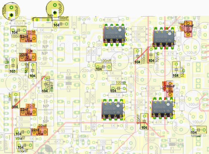
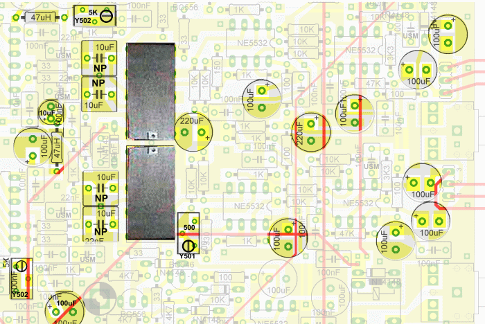
Install NPO and USM Capacitors
Install the ceramic capacitors (and the two "boundary" 100 uF electrolytics).
Note that there are two types of ceramic capacitors here: the normal 103s and 104s and the larger "USM" capacitors which are colored differently.
| Check | Designation | Component | Marking | Category | Orientation | Notes |
|---|---|---|---|---|---|---|
| ❏ | C5-1 | 22 nF USM | F98 223J or F87 223J
| Metalized polyfilm | annotated "USM" on the graphic | |
| ❏ | C5-2 | 22 nF USM | F98 223J or F87 223J
| Metalized polyfilm | annotated "USM" on the graphic | |
| ❏ | C5-3 | 22 nF USM | F98 223J or F87 223J
| Metalized polyfilm | annotated "USM" on the graphic | |
| ❏ | C5-4 | 22 nF USM | F98 223J or F87 223J
| Metalized polyfilm | annotated "USM" on the graphic | |
| ❏ | C5-99 | 10 nF (.01uF) | 103
| Ceramic | ||
| ❏ | C5-10 | 100 nF | 104
| Ceramic | ||
| ❏ | C5-11 | 100 nF | 104
| Ceramic | ||
| ❏ | C5-12 | 100 nF | 104
| Ceramic | ||
| ❏ | C5-13 | 100 nF | 104
| Ceramic | ||
| ❏ | C5-14 | 100 nF | 104
| Ceramic | ||
| ❏ | C5-15 | 100 nF | 104
| Ceramic | ||
| ❏ | C5-16 | 100 nF | 104
| Ceramic | ||
| ❏ | C5-17 | 100 nF | 104
| Ceramic | ||
| ❏ | C5-18 | 100 nF | 104
| Ceramic | ||
| ❏ | C5-19 | 100 nF | 104
| Ceramic | ||
| ❏ | C5-20 | 100 nF | 104
| Ceramic | ||
| ❏ | C5-5 | 100 nF USM | 104J
| Metalized polyfilm | annotated "USM" on the graphic | |
| ❏ | C5-6 | 100 nF USM | 104J
| Metalized polyfilm | annotated "USM" on the graphic | |
| ❏ | C5-7 | 100 nF | 104
| Ceramic | ||
| ❏ | C5-8 | 100 nF | 104
| Ceramic | ||
| ❏ | C5-9 | 100 nF | 104
| Ceramic | ||
| ❏ | C5-39 | 100 uF/25Vdc |
| Electrolytic | ||
| ❏ | C5-40 | 100 uF/25Vdc |
| Electrolytic |
Install Ics
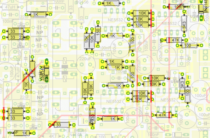
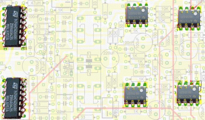
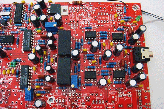
Install the 4 OpAmp Ics (using ESD precautions and taking care to orient them correctly - see the graphic above). The Ics are oriented so that their "1" pins are in the upper right, when viewing the board with the Power supply at the top.
| Check | Designation | Component | Marking | Category | Orientation | Notes |
|---|---|---|---|---|---|---|
| ❏ | U5-1 | 74HC4066 Quad Bilateral SW |
| DIP-14 | Take ESD precautions | |
| ❏ | U5-2 | 74HC4066 Quad Bilateral SW |
| DIP-14 | Take ESD precautions | |
| ❏ | U5-3 | NE5532 Dual OpAmp | NE5532
| DIP-8 | Pin 1 is to upper right | Take ESD precautions |
| ❏ | U5-4 | NE5532 Dual OpAmp | NE5532
| DIP-8 | Pin 1 is to upper right | Take ESD precautions |
| ❏ | U5-5 | NE5532 Dual OpAmp | NE5532
| DIP-8 | Pin 1 is to upper right | Take ESD precautions |
| ❏ | U5-6 | NE5532 Dual OpAmp | NE5532
| DIP-8 | Pin 1 is to upper right | Take ESD precautions |
Install Remaining Components
Prior to installing the Y502 trimpots, check their resistance; each leg should have 2.5kOhms - i.e., the trimpots should be set exactly in the middle of the 5kOhm range. This should be the factory setting, but it does not hurt to check just in case these may have been jostled in shipment/handling. These trimpots will later be used for TX carrier suppression adjustments, if any. They are will be adjusted in this phase (and in the Final Tests and Adjustments page).
Note that there are 4 "can-like" capacitors that can easily be confused as polarized electrolytic capacitors. However, there 4 10 uF capacitors are NON-polarized ("NP"), with no need to be concerned about + and minus otientations. There is another 10uF capacitor that is polarized. Do not get the 2 types confused! All of the polarized electrolytics have that grey stripe with the minus sign down the side; the "NP" capacitors do not have that stripe. Refer to the BOM for visuals.
| Check | Designation | Component | Marking | Category | Orientation | Notes |
|---|---|---|---|---|---|---|
| ❏ | R5-38 | 500 (Y501) | Y501
| Trimpot | ||
| ❏ | R5-39 | 5K (Y502) | Y502
| Trimpot | Needs to be initialized (see notes above) | |
| ❏ | R5-40 | 5K (Y502) | Y502
| Trimpot | Needs to be initialized (see notes above) | |
| ❏ | L5-1 | 47 uH molded inductor 10% | yel-vio-blk-slv
| Choke | ||
| ❏ | L5-2 | 47 uH molded inductor 10% | yel-vio-blk-slv
| Choke | ||
| ❏ | C5-35 | 10 uF (NP) |
| Non-Polarized | Don't confuse with 10 uF electrolytic | |
| ❏ | C5-36 | 10 uF (NP) |
| Non-Polarized | Don't confuse with 10 uF electrolytic | |
| ❏ | C5-37 | 10 uF (NP) |
| Non-Polarized | Don't confuse with 10 uF electrolytic | |
| ❏ | C5-38 | 10 uF (NP) |
| Non-Polarized | Don't confuse with 10 uF electrolytic | |
| ❏ | K5-1 | JRC27F/012 relay | JRC27F/012
| 12V relay | ||
| ❏ | K5-2 | JRC27F/012 relay | JRC27F/012
| 12V relay | ||
| ❏ | C5-22 | 10 uF/25Vdc |
| Electrolytic | Don't confuse with 10 uF non-polarized ("NP") | |
| ❏ | C5-23 | 100 uF/25Vdc |
| Electrolytic | ||
| ❏ | C5-24 | 100 uF/25Vdc |
| Electrolytic | ||
| ❏ | C5-25 | 100 uF/25Vdc |
| Electrolytic | ||
| ❏ | C5-26 | 100 uF/25Vdc |
| Electrolytic | ||
| ❏ | C5-27 | 100 uF/25Vdc |
| Electrolytic | ||
| ❏ | C5-28 | 100 uF/25Vdc |
| Electrolytic | ||
| ❏ | C5-29 | 100 uF/25Vdc |
| Electrolytic | ||
| ❏ | C5-30 | 100 uF/25Vdc |
| Electrolytic | ||
| ❏ | C5-31 | 100 uF/25Vdc |
| Electrolytic | ||
| ❏ | C5-32 | 100 uF/25Vdc |
| Electrolytic | ||
| ❏ | C5-33 | 220 uF/25Vdc |
| Electrolytic | ||
| ❏ | C5-34 | 220 uF/25Vdc |
| Electrolytic |
Install Connectors
| Check | Designation | Component | Marking | Category | Orientation | Notes |
|---|---|---|---|---|---|---|
| ❏ | P5-1 | 3.5mm stereo jack - PCB mount (rt-angle) |
| Jack-RA | ||
| ❏ | P5-2 | BNC Connector Male - PCB mount |
| Jack | Careful: there are two places for BNC. This one goes in the lower location |
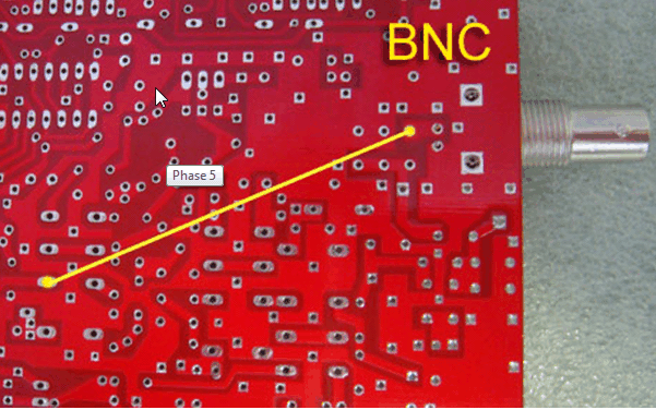
Temporarily Connect Antenna And Mixer Input
Tack-solder a wire to connect the antenna "hot" pin on the BNC connector to the Mixer Stage's Input point on the board, as indicated in the graphic.
Builder may choose to install this temporary wire from the bottom or from the top:
(This wire will be removed in the next phase.)
Installing from Topside
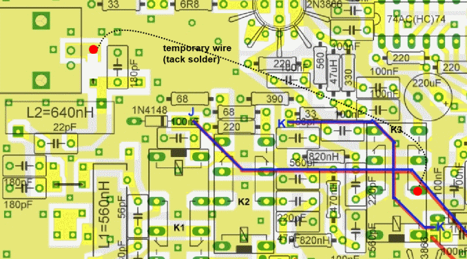
Installing from Bottomside
| Check | Designation | Component | Marking | Category | Orientation | Notes |
|---|---|---|---|---|---|---|
| ❏ | TMP5-1 | misc hookup wire | Hookup | temporary connection |
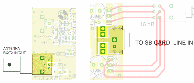
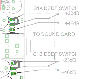
Temporarily enable IQ Output
Temporarily connect the pins for switches S1A and S1B, to enable I and Q output to the ("To Sound Card") stereo jack. This involves shorting together pins 3 and 2 in each of the two sets of holes flanking the jack (i.e., simulating the setting of the switches to the 23dB position).
The two switches attached to this stage are:
- Preamp gives an additional 15 dB of gain in the RF input. Probably only needed on 20 meters.
- Attenuator is self-evident. It’s purpose is to allow the radio to function in a very intense RF environment. Rarely needed.
| Check | Designation | Component | Marking | Category | Orientation | Notes |
|---|---|---|---|---|---|---|
| ❏ | tsw1_2 | shunt wire (cut-off lead) | Cutoff | temporary connection - see diagram |
RX Mixers/OpAmps Testing
NE5532 Pin Voltages
Test Setup
Apply 12 - 13.8 Vdc power to the board and measure, in turn, the pin voltages on each NE5532
Each should yield the following pin voltages:
- Pins 1, 2, 3, 5, 6, and 7: +6Vdc
- Pin 4: (gnd) 0 Vdc
- Pin 8: = Vin = 12Vdc
The 6 Vdc reading above is nominal and will actually depend upon your power source. Some will use 13.8 Vdc; some may have just 12V dc (as in the typical gel cell). The important thing is that the voltages (nominally 6V dc) must be the same on each of the indicated pins.
Test Measurements
| Testpoint | Units | Nominal Value | Author's | Yours |
|---|---|---|---|---|
| Each NE5532: pins 1, 2, 3, 5, 6, and 7 | V dc | +6 | tdb | _______ |
| Each NE5532: pin 4 | V dc | 0 | tdb | _______ |
| Each NE5532: pin 8 | V dc | +12 | tdb | _______ |
Image Adjustment
Test Setup
At this stage it is absolutely essential to ensure that both I and Q channels are working properly and image rejection is adjusted (-40dB or better).
"Images" are a common artifact of the Direct Conversion receiver which is the basis for this SDR. They are encountered in the display when:
- the phasing of the I and Q signals is not just right; OR
- when only one of the two signals is present, either because of a bad connection or a mono soundcard input).
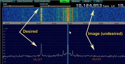
Images are pretty obvious on the spectrum display of the SDR, looking like mirror inage signals on either side of the center frequency. One of these is the desired signal; the other is an image that should be rejected. For example, if the center frequency is 10.125 MHz and your desired signal is 10.135 MHz (10 kHz above the center "zero"), then there may be a mirror image of that signal at 10.115 kHz (10 kHz below the center "zero"). Adjusting for image rejection causes these unwanted images to disappear down into the noise level.
To begin, Download and setup Winrad to serve as a SDR receiving program (you may prefer, instead, to use the GSDR program - Hans, LA2MOA's setup instructions are here.
Image adjustment will require a running SDR program tuned to one of the center frequencies and a signal source that is slightly above or below that center frequency. For this example, we will use the 30m center frequency of 10.125 MHz and a signal source of 10.115 MHz (10 kHz below the center). Preston, WJ2V, has found that if the test signal was too large, it was picked up in the unshielded G3020, and it would not suppress! Use a small signal to do these tests. When Preston got the signal down to proper levels for receive testing, the supression worked like magic.
The adjustment procedure below is extracted from Preston's excellent FAQAdjustment Procedure
The G3020 has four pots that must be adjusted to balance the audio lines for proper operation.
Set Up Sound Card
Start up your Genesis software, and connect your sound card to the G3020:- Connect line In of PC to the "To PC Soundcard" jack on the G3020 board
- Do not connect the soundcard's line out to the G3020 yet
Signal Source
You will need a source of low signal in either the 30 or 20 meter bands. You must keep the signal level quite low or the Genesis will be overloaded, and you won’t see the nulls you are looking for. Builders have reported inability to find a null when the signal strength is too high. For example, you may have trouble with a standard 100 watt rig connected to a dummy load—the escaped signal may still be pretty high. If necessary, move your G3020 away from the signal source. Of course, a signal generator would be ideal, but it isn’t necessary.
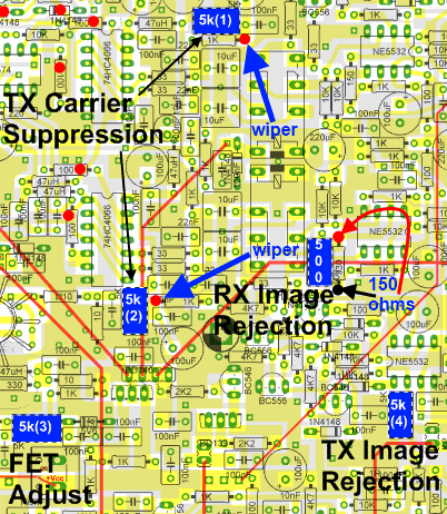
Adjust Carrier Trim Pots
Now, look at the above graphic. If you printed this out in advance, it will be easier than trying to look at your computer while you work. Note there are two 5k (Y503) trim pots labeled "TX Carrier Suppression". These pots must be pre-adjusted. Locate them on your board, so you are oriented.
- Power the board so you can make some voltage measurements with respect to ground (WRTG)
- You will find that the trimmer pot at the top of your board has a 1K resistor right below it. The right side of this resistor (red dot) is connected to the wiper of this trimmer. Adjust that trim pot to exactly 2.50 volts (WRTG) with power on the board.
- Now go to the second Carrier Null trimmer. The wiper of this trimmer is connected to the left side (red dot) of the 1K resistor just to the right of the trimmer. Adjust this second trimmer for 2.50 volt (WRTG) as well.
- Note that although these two pots are ultimately used to null out the carrier, they must be very close to equal, or you will not be able to suppress the image in the receiver.
RX Image Adjustment
Next trimmer is the 500 ohm (Y502) receiver image adjustment trimmer, for which you will need a small signal. Staying with our 30m example, your G3020 uses a local oscillator at 10.125 MHz. If you generate a signal at 10.115, which is 10K below the LO center, the image will be on 10.135, 10K above. If you generate a signal at 10.135, the image is on the other side, i.e. 10.115.
So, now look at your SDR software's spectrum display onm the PC and note the two signals, the correct signal, and the wrong side image.
Turn power OFF. Referring to the trimmer adjustment graphic find the receive image suppression pot. With power off, pre-set it so that the resistance across the 330 ohm resistor (to the right of the pot) is 150 ohms, as shown in the above graphic
Once your image suppression pot is pre-adjusted, you can carefully turn it until the image starts to drop. It should show at least 30dB, more likely 40dB of null. If the wrong signal is dropping, go in to the your SDR software's setup, and reverse the receive I/Q lines to correct this problem. Now, the image should be suppressed.
Turn the power on, fire up your SDR software for the G3020 and start up your signal source. Then, adjust the image reject trimmer while observing the "image" signal on the spectrum display. Refer to the procedure outlined for the G40 kit's image adjustment to see what the image rejection process looks like. You will be using different input frequency with your G3020, but the rest of the instructions apply. You can also get a very good idea of how this works by viewing the You Tube video by Josh, Vk2FJDX (fast forward to minute 4:40).
Also, you might find that the Genesis software is easier to use than others.
Watch One Work
Test Setup
Here is a Youtube video of Brian KJ4OOS' Genesis G3020 receiving SSB signals at the end of this Phase: