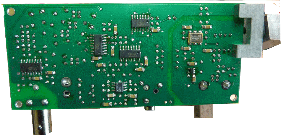
Operational Amplifiers Introduction
(go directly to build notes)Operational Amplifiers Schematic
(Resistor testpoints (hairpin, top, or left-hand lead), as physically installed on the board, are marked in the schematic with red dots)
(Click for Full Schematic)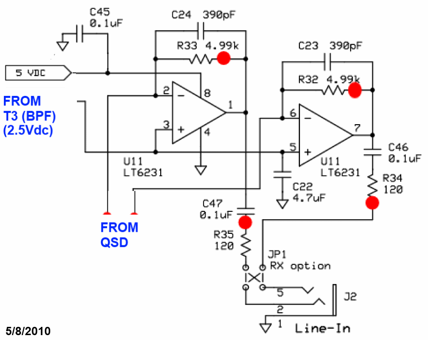
(above schematic has clickable areas that can be used for navigation)
(go directly to build notes)Operational Amplifiers Bill of Materials
Stage Bill of Materials
(resistor images and color codes courtesy of WIlfried, DL5SWB's R-Color Code program)
| Check | Count | Component | Marking | Category |
|---|---|---|---|---|
| ❏ | 2 | 4.99 k 1/4W 1% | y-w-w-br-br
 | 1/4W |
| ❏ | 2 | 120 1/6W 5% | brn-red-brn-gld
 | 1/6W |
| ❏ | 2 | 390 pF 5% | 391
 | Ceramic |
| ❏ | 1 | 4.7 uF 10% 16V X7R RAD | 475
 | Ceramic |
| ❏ | 2 | misc hookup wire | Hookup | |
| ❏ | 1 | 3.5mm stereo jack - PCB mount (rt-angle) |
 | Jack-RA |
| ❏ | 3 | 0.1 uF | (smt) black stripe
 | SMT 1206 |
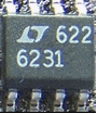
| ❏ | 1 | LT6231 dual op-amp | LT6231
 | SOIC-8 |
Operational Amplifiers Summary Build Notes
- Install Bottomside Parts
- Install Topside Parts
- Test the Stage
Operational Amplifiers Detailed Build Notes
Top of the Board
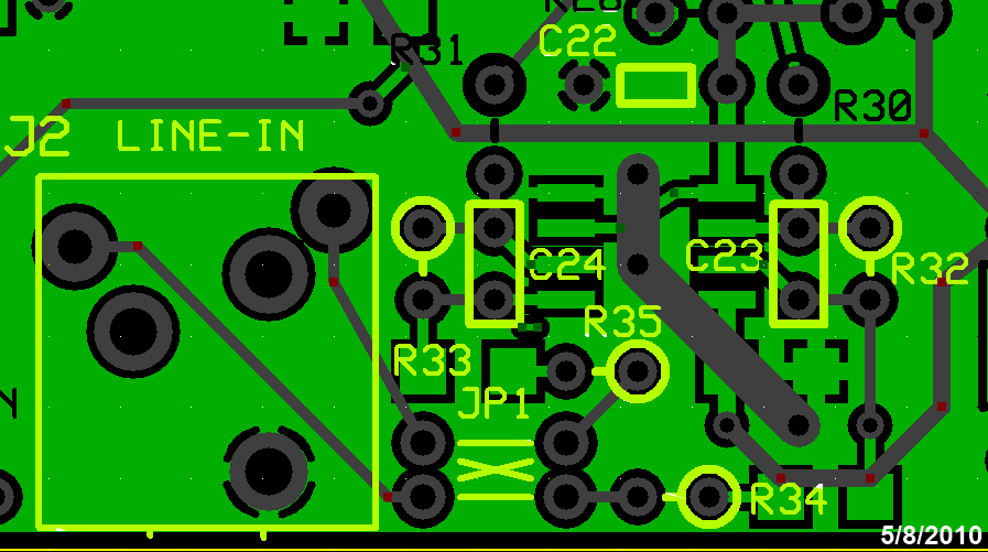
Install Topside Parts
Careful - there are 1/6W and 1/4W resistors in this step.
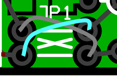
When installing the jumpers to the line-in jack, the builder is advised to install them crosswise (i.e., in the "X" pattern), rather than straight (in the parallel pattern), using insulated hookup wire to avoid shorts. This will make the receiver adaptable to all currently published SDR software. While the outputs would appear reversed to Rocky and Winrad, those two programs have a programmatic "switch I and Q lines" setting that can compensate. The PSDR versions do not have such a setting.
| Check | Designation | Component | Marking | Category | Orientation | Notes |
|---|---|---|---|---|---|---|
| ❏ | C22 | 4.7 uF 10% 16V X7R RAD | 475
| Ceramic | horiz | |
| ❏ | C24 | 390 pF 5% | 391
| Ceramic | vert | |
| ❏ | C23 | 390 pF 5% | 391
| Ceramic | vert | |
| ❏ | R32 | 4.99 k 1/4W 1% | y-w-w-br-br
| 1/4W | N-S | |
| ❏ | R33 | 4.99 k 1/4W 1% | y-w-w-br-br
| 1/4W | N-S | |
| ❏ | R34 | 120 1/6W 5% | brn-red-brn-gld
| 1/6W | E-W | |
| ❏ | R35 | 120 1/6W 5% | brn-red-brn-gld
| 1/6W | E-W | |
| ❏ | JP1A | misc hookup wire | Hookup | |||
| ❏ | JP1B | misc hookup wire | Hookup | |||
| ❏ | J02 | 3.5mm stereo jack - PCB mount (rt-angle) |
| Jack-RA |
Bottom of the Board
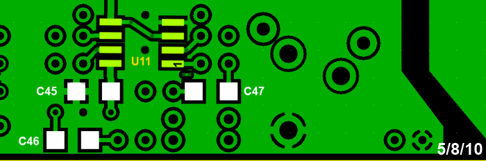
Install Bottomside Parts
| Check | Designation | Component | Marking | Category | Orientation | Notes |
|---|---|---|---|---|---|---|
| ❏ | U11 | LT6231 dual op-amp | LT6231
| SOIC-8 | (or LT6221) | Take ESD precautions |
| ❏ | C45 | 0.1 uF | (smt) black stripe
| SMT 1206 | white pads | |
| ❏ | C46 | 0.1 uF | (smt) black stripe
| SMT 1206 | white pads | |
| ❏ | C47 | 0.1 uF | (smt) black stripe
| SMT 1206 |
Operational Amplifiers Completed Stage
Top of the Board
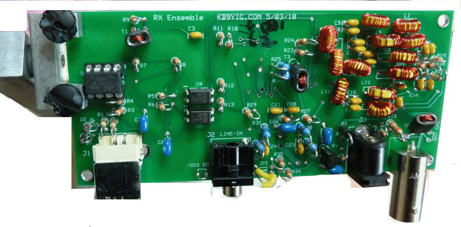
Bottom of the Board
Operational Amplifiers Testing
Pin Voltage Tests
Test Setup
Test pin voltages WRT regular ground, as per graphic
As usual, if you are having any problems with this stage, be sure to measure the pin voltages two ways: first, measure each pin at the pin itself (on the IC). Then take a second measurement at the pin pad (on the board). If those two measurements do NOT agree, you very likely have a soldering issue.
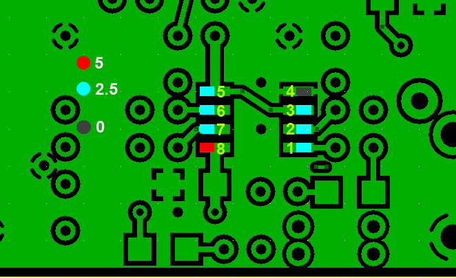
Test Measurements
| Testpoint | Units | Nominal Value | Author's | Yours |
|---|---|---|---|---|
| Pin 1 (50% of 5V rail) | V dc | 2.5 | 2.45 | _______ |
| Pin 2 (50% of 5V rail) | V dc | 2.5 | 2.43 | _______ |
| Pin 3 (50% of 5V rail) | V dc | 2.5 | 2.43 | _______ |
| Pin 4 (gnd) | V dc | 0 | 0 | _______ |
| Pin 5 (50% of 5V rail) | V dc | 2.5 | 2.43 | _______ |
| Pin 6 (50% of 5V rail) | V dc | 2.5 | 2.43 | _______ |
| Pin 7 (50% of 5V rail) | V dc | 2.5 | 2.46 | _______ |
| Pin 8 (5V rail) | V dc | 5 | 4.92 | _______ |
Functional Test
Test Setup
Test Setup
In this test, you will test the DC gain of each of the op-amps by connecting a bridging resistor Rb from each op-amp inverting input to circuit regular ground. Introducing the "bridging" resistor Rb will result in a test current equal to 2.5 / Rt, which will be balanced by the current fed back from each op-amp's output through each feedback resistor, Rf (i.e., R33 or R32). Each op-amp output will increase in voltage by 2.5 * Rf/ Rb from the nominal DC level of 2.5 volts.
You will need to obtain a 10k resistor from your junk box or other source for this test.
Test the First OpAmp
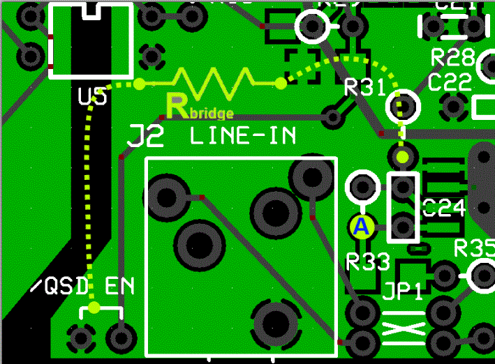
- Power up the circuit and measure the voltage at pin 1 of the op-amp (hairpin of R33). It should be ~2.5 Vdc
- Power off and use clip leads to connect Rb between the hairpin of R31 and circuit ground. This provides an input resistance(Ri) of 10 kΩ, to the op-amp.
- Power up and measure the output voltage (WRT regular ground) at the hairpin of the feedback resistor R33. You should get ~3.75 Vdc at R33 hairpin.
- Remove Rb and the output voltage at R33 should go back to ~2.5 Vdc.
Test the Second OpAmp
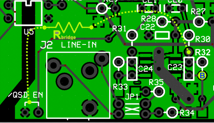
- Power up the circuit and measure the voltage at pin 1 of the op-amp (hairpin of R32). It should be ~2.5 Vdc
- Power off and use clip leads to connect Rb between the hairpin of R30 and circuit ground. This provides an input resistance(Ri) 10 kΩ, to the op-amp.
- Power up and measure the output voltage (WRT regular ground) at the hairpin of the feedback resistor R32. You should get: ~3.75 Vdc at R32 hairpin.
- Remove Rb and the output voltage at R32 should go back to ~2.5 Vdc.
The diagram below shows the test points. The yellow dots show the Rb connection points for each "side" of the opamps. The dots marked "A" and "B" show the measurement points for the output voltages for Each "side" of the OpAmps.
An Excel spreadsheet with a calculator for this test is available for you to plug in your bridging resistor ohms (Rt) and your pin 1 or pin 7 normal voltages (Ebias) and predict the expected voltage when bridged (Eout).Test Measurements
| Testpoint | Units | Nominal Value | Author's | Yours |
|---|---|---|---|---|
| "A" (hairpin lead of R33 (NOT bridged) | V dc | 2.5 | 2.45 | _______ |
| "A" (hairpin lead of R33 (bridged) | V dc | 3.75 | 3.66 | _______ |
| "B" (hairpin lead of R32 (NOT bridged) | V dc | 2.5 | 2.46 | _______ |
| "B" (hairpin lead of R32 (bridged) | V dc | 3.75 | 3.68 | _______ |
RX Test
Test Setup
Prepare an SDR program for RX (author recommends Rocky for the Windows XP crowd; WinradHD for other Windows OS). This usually involves downloading and installing the program; selecting the desired soundcard for the (STEREO) input of the I and Q signals from the board; and connecting the board to the soundcard with a stereo cable with 1/8" stereo plugs on either end..
Once the SDR program is ready, connect the USB cable from your PC to the board, connect the 12V power to the board, and connect a 50 ohm antenna to J4.
Start the SDR program and adjust the LO frequency to the desired center frequency. You should see signals in the displayed spectrum. If there is a contest going on at test time, you will be even more impressed with the RX.!
Note: for either SDR program to work with the Ensemble RX, you MUST have installed the driver (libusb) for the Microcontroller's USB functionality. For WinradHD, you will also need to have downloaded and saved in the same directory as WinradHD, the EXTIO_Si570.dll file.
If you are seeing perfect mirror inages of the signals either side of the center frequency, you should review the information in the Image Rejection Hints page.
If you installed the I/Q jumpers as suggested, you will need (in Rocky and/or Winrad) to switch the I and Q inputs to get signals properlay arrayed on the correct "side" of the center frequency.
Note that there is an optional grounding via for the return side of the antenna connection. Normally, you would want to ground this to regular circuit ground. However, if you encounter significant ground loop problems, you may want to un-ground the antenna shield side.