Operational Amplifiers Introduction
General
This stage accepts, as input, the Quadrature Sampling Detected "chunk" of spectrum containing the signals occurring either side of the center frequency set by the Quadrature Clock Generator (Dividers). This "chunk" is in the base-band, at frequencies ranging from zero to (roughly) 100 kHz or so. There are "I" (In-Phase) and a "Q" (Quadrature) signals, each identical in all respects except phase (90 degrees difference). The "I" and "Q" signals are amplified in this high-gain op-amp and output to the "Line-In" jack for input to the PC's soundcard's "Line-In" jack. For the 2m option, jumpers JP1A and JP1B can be wired straight through (rather than crossed). For the bands below 2m (i.e., 6m and, in the EU, 4m) the LO frequency will be higher than the desired VHF frequency. This calls for swapping the I and Q leads from their normal ring/tip orientation by cross-wiring JO1A and JP1B .
A very important aspect of this latter is that the PC's soundcard MUST be capable of accepting STEREO inputs. If the input to the soundcard is MONO, the radio will not work correctly, and you will see identical, "mirror" images on either side of the center frequency in the spectrum display of the SDR program.
At the completion of this stage, you should have and be able to exercise RX capability!.
(go directly to build notes)Operational Amplifiers Schematic
(Resistor testpoints (hairpin, top, or left-hand lead), as physically installed on the board, are marked in the schematic with red dots)
(above schematic has clickable areas that can be used for navigation)
(go directly to build notes)Operational Amplifiers Bill of Materials
Stage Bill of Materials
(resistor images and color codes courtesy of WIlfried, DL5SWB's R-Color Code program)
| Check | Designation | Component | Marking | Category | Orientation | Notes | Circuit |
|---|---|---|---|---|---|---|---|
| ❏ | C19 | 4.7 uF 10% 16V X7R RAD | 475
 | Ceramic | Operational Amplifiers | ||
| ❏ | C20 | 390 pF 5% | 391
 | Ceramic | Operational Amplifiers | ||
| ❏ | C21 | 390 pF 5% | 391
| Ceramic | Operational Amplifiers | ||
| ❏ | R23 | 4.99 k 1/4W 1% | y-w-w-br-br
 | 1/4W | Operational Amplifiers | ||
| ❏ | R24 | 4.99 k 1/4W 1% | y-w-w-br-br
| 1/4W | Operational Amplifiers | ||
| ❏ | R25 | 120 1/6W 5% | brn-red-brn-gld
 | 1/6W | Operational Amplifiers | ||
| ❏ | R26 | 120 1/6W 5% | brn-red-brn-gld
| 1/6W | Operational Amplifiers | ||
| ❏ | JP1A | shunt wire (cut-off lead) | Cutoff | Operational Amplifiers | |||
| ❏ | JP1B | shunt wire (cut-off lead) | Cutoff | Operational Amplifiers | |||
| ❏ | J02 | 3.5mm stereo jack - PCB mount (rt-angle) |
 | Jack-RA | Operational Amplifiers | ||
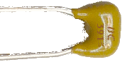
| ❏ | U09 | LT6231 dual op-amp | LT6231
 | SOIC-8 | (or LT6221) | Operational Amplifiers | |
| ❏ | C45 | 0.1 uF | (smt) black stripe
 | SMT 1206 | Operational Amplifiers | ||
| ❏ | C46 | 0.1 uF | (smt) black stripe
| SMT 1206 | Operational Amplifiers | ||
| ❏ | C47 | 0.1 uF | (smt) black stripe
| SMT 1206 | Operational Amplifiers | ||
| ❏ | Rb | 10 k Test Resistor | User-Supplied | Operational Amplifiers |
Operational Amplifiers Summary Build Notes
- Install SMT Components
- Install Topside Components
- Install I/Q Jumpers and Jack
- Test the Stage
Operational Amplifiers Detailed Build Notes
Bottom of the Board
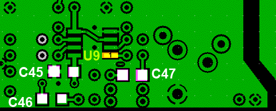
Install SMT Components
| Check | Designation | Component | Marking | Category | Orientation | Notes |
|---|---|---|---|---|---|---|
| ❏ | U09 | LT6231 dual op-amp | LT6231
| SOIC-8 | (or LT6221) | Take ESD precautions |
| ❏ | C45 | 0.1 uF | (smt) black stripe
| SMT 1206 | ||
| ❏ | C46 | 0.1 uF | (smt) black stripe
| SMT 1206 | ||
| ❏ | C47 | 0.1 uF | (smt) black stripe
| SMT 1206 |
Top of the Board
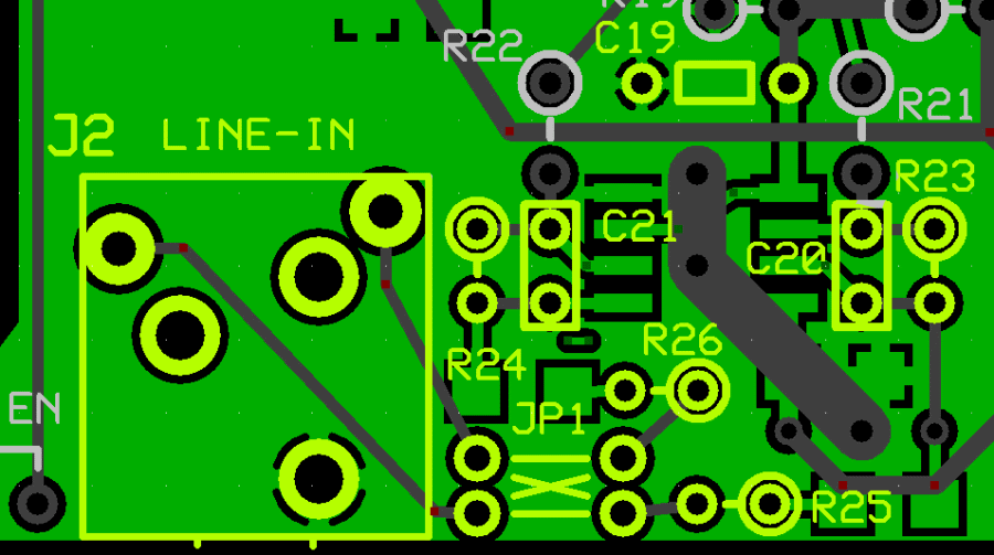
Install Topside Components
| Check | Designation | Component | Marking | Category | Orientation | Notes |
|---|---|---|---|---|---|---|
| ❏ | C19 | 4.7 uF 10% 16V X7R RAD | 475
| Ceramic | ||
| ❏ | C20 | 390 pF 5% | 391
| Ceramic | ||
| ❏ | C21 | 390 pF 5% | 391
| Ceramic | ||
| ❏ | R23 | 4.99 k 1/4W 1% | y-w-w-br-br
| 1/4W | ||
| ❏ | R24 | 4.99 k 1/4W 1% | y-w-w-br-br
| 1/4W | ||
| ❏ | R25 | 120 1/6W 5% | brn-red-brn-gld
| 1/6W | ||
| ❏ | R26 | 120 1/6W 5% | brn-red-brn-gld
| 1/6W |
Install I/Q Jumpers and Jack
For the 2m option, jumpers JP1A and JP1B can be wired straight through (rather than crossed). For the bands below 2m (i.e., 6m and, in the EU, 4m) the LO frequency will be higher than the desired VHF frequency. This calls for swapping the I and Q leads from their normal ring/tip orientation by cross-wiring JO1A and JP1B .
| Check | Designation | Component | Marking | Category | Orientation | Notes |
|---|---|---|---|---|---|---|
| ❏ | JP1A | shunt wire (cut-off lead) | Cutoff | |||
| ❏ | JP1B | shunt wire (cut-off lead) | Cutoff | |||
| ❏ | J02 | 3.5mm stereo jack - PCB mount (rt-angle) |
| Jack-RA |
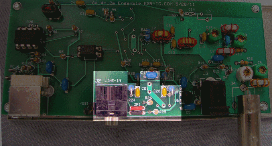
Operational Amplifiers Completed Stage
Top of the Board
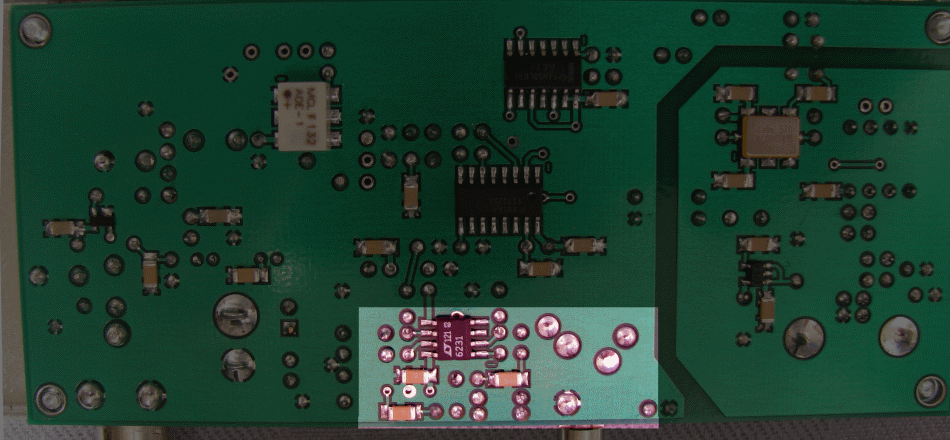
Bottom of the Board
Operational Amplifiers Testing
Pin Voltages
Test Setup
The 2.5V pins get their voltages from the voltage divider that was installed in the RF/Control Stage
Test pin voltages WRT regular ground, as per graphic (Some of the pins can be quick-tested from the top of the board by probing the specified hairpin leads. If there is any question, doubt, or issue, however, you should do the pins and pads testing from the bottomside.)
As usual, if you are having any problems with this stage, be sure to measure the pin voltages two ways: first, measure each pin at the pin itself (on the IC). Then take a second measurement at the pin pad (on the board). If those two measurements do NOT agree, you very likely have a soldering issue.
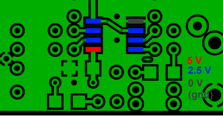
Test Measurements
| Testpoint | Units | Nominal Value | Author's | Yours |
|---|---|---|---|---|
| Pin 1 (R24 hairpin) | V dc | 2.5 | _______ | |
| Pin 2 (R22 hairpin) | V dc | 2.5 | _______ | |
| Pin 3 | V dc | 2.5 | _______ | |
| Pin 4 | V dc | 0 | _______ | |
| Pin 5 | V dc | 2.5 | _______ | |
| Pin 6 (R21 hairpin) | V dc | 2.5 | _______ | |
| Pin 7 (R23 hairpin) | V dc | 2.5 | _______ | |
| Pin 8 (R18 hairpin) | V dc | 5 | _______ |
Functional Test
Test Setup
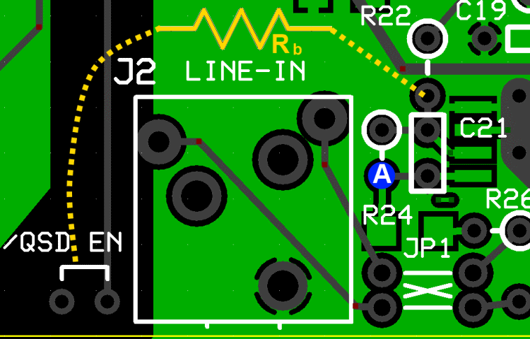
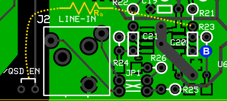
In this test, you will test the DC gain of each of the op-amps by connecting a bridging resistor Rb from each op-amp inverting input to circuit regular ground.
Introducing the "bridging" resistor Rb will result in a test current equal to 2.5 / Rt, which will be balanced by the current fed back from each op-amp's output through each feedback resistor, Rf (i.e., R23 or R24). Each op-amp output will increase in voltage by 2.5 * Rf/ Rb from the nominal DC level of 2.5 volts.
You will need to obtain a 10k resistor from your junk box or other source for this test.
Test the First OpAmp
- Power up the circuit and measure the voltage at pin 1 of the op-amp (hairpin of R24). It should be ~2.5 Vdc
- Power off and use clip leads to connect Rb between the hairpin of R22 and circuit ground. This provides an input resistance(Ri) of 10 kOhm, to the op-amp.
- Power up and measure the output voltage (WRT regular ground) at the hairpin of the feedback resistor R24. You should get ~3.75 Vdc at R24 hairpin.
- Remove Rb and the output voltage at R24 should go back to ~2.5 Vdc.
Test the Second OpAmp
- Power up the circuit and measure the voltage at pin 7 of the op-amp (hairpin of R23). It should be ~2.5 Vdc
- Power off and use clip leads to connect Rb between the hairpin of R21 and circuit ground. This provides an input resistance(Ri) 10 kOhm, to the op-amp.
- Power up and measure the output voltage (WRT regular ground) at the hairpin of the feedback resistor R23. You should get: ~3.75 Vdc at R23 hairpin.
- Remove Rb and the output voltage at R23 should go back to ~2.5 Vdc.
An Excel spreadsheet with a calculator for this test is available for you to plug in your bridging resistor ohms (Rt) and your pin 1 or pin 7 normal voltages (Ebias) and predict the expected voltage when bridged (Eout).
Test Measurements
| Testpoint | Units | Nominal Value | Author's | Yours |
|---|---|---|---|---|
| "A" (hairpin lead of R22 (NOT bridged) | V dc | 2.5 | _______ | |
| "A" (hairpin lead of R22 (bridged) | V dc | 3.75 | _______ | |
| "B" (hairpin lead of R23 (NOT bridged) | V dc | 2.5 | _______ | |
| "B" (hairpin lead of R23 (bridged) | V dc | 3.75 | _______ |