RX OpAmps Introduction
General
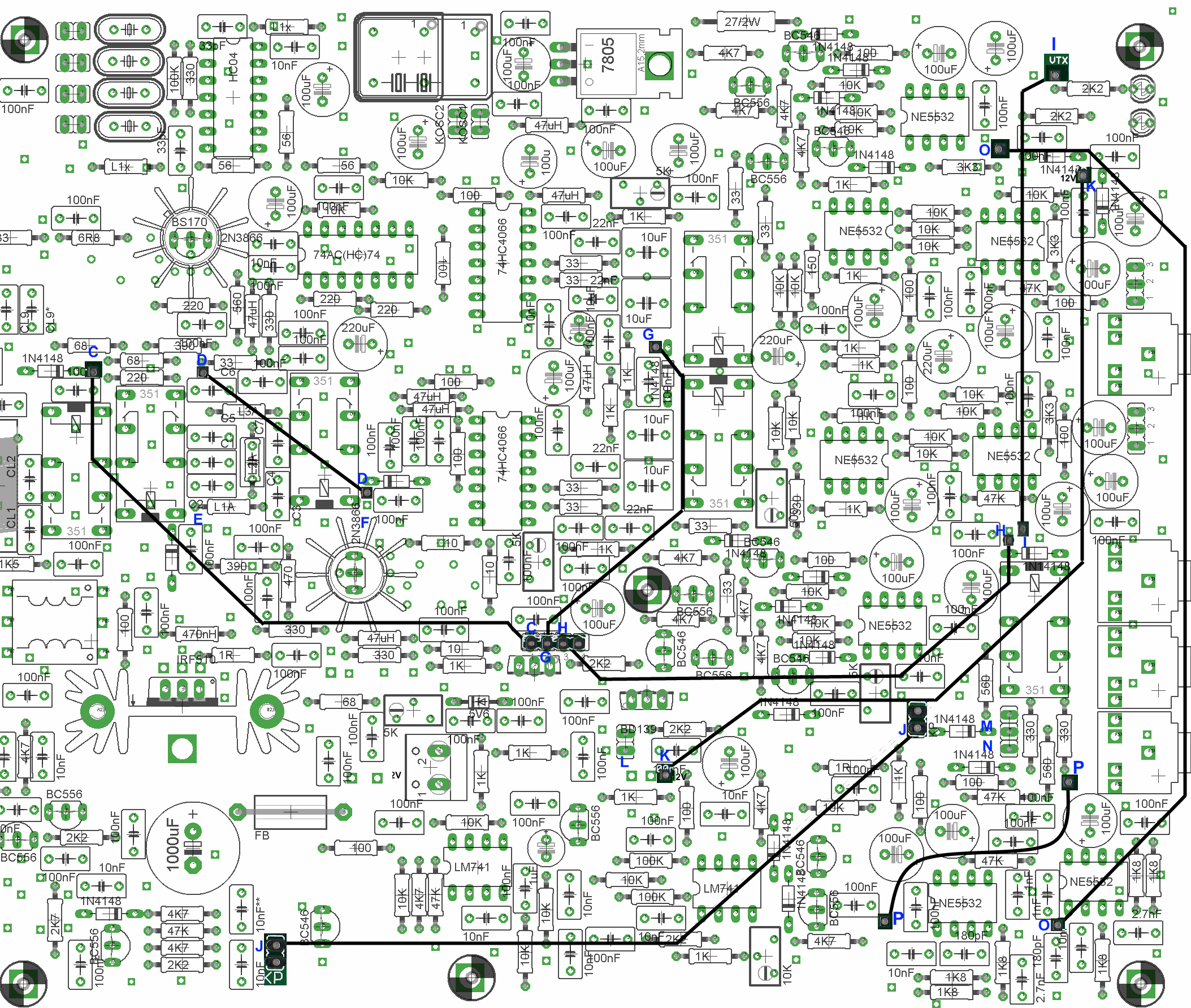
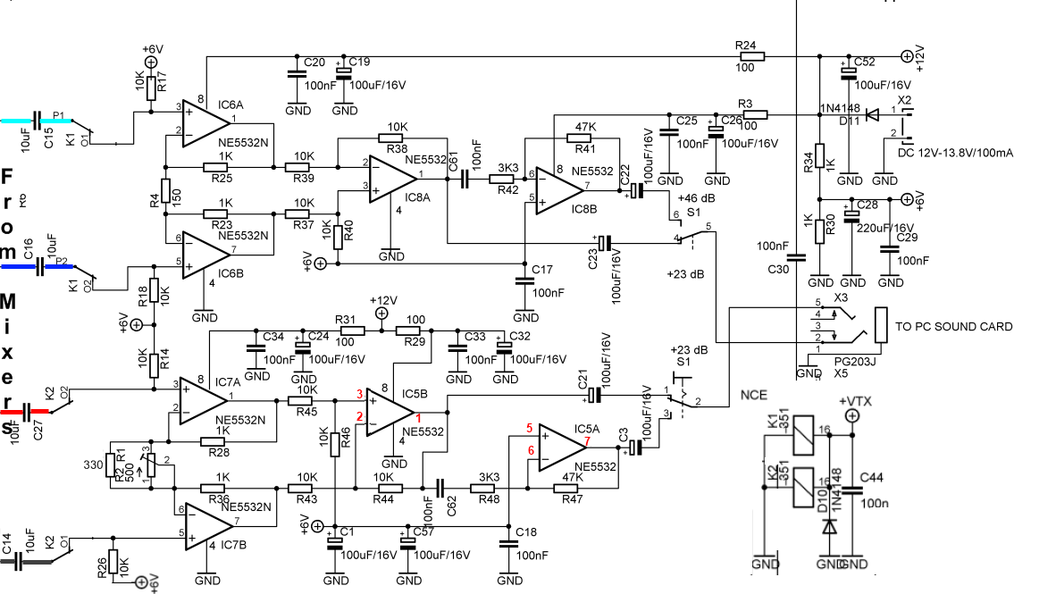
In this phase, the down-converted audio frequency signals (in quadrature) from the mixersare combined (0° + 180°, 90° + 270 °) and then summed and passed to the PC, either directly following the summing operatikon or passed through an amplification stage for a 23 db boost (as determined by S1), as I and Q outputs of the G40.
The sub-schematic below shows the RX path for the opamps. (A similar path is defined for the TX opamps, where the I and Q signals from the PC are sent to the mixers and out to the RF line.) The relays, designated in the schematic below as K1 and K2, act to switch the I/Q signal pairs from the default RX to the TX signals when activated by the voltage at Vtx. Vtx is present when the PTT is activated via the RX/TX Control circuitry. In the final wiring diagram, this Vtx is provided by a wire whose end-points are identified by the letter "G". In the final wiring diagram.
RX OpAmps Schematic
RX OpAmps Bill of Materials
Stage Bill of Materials
(resistor images and color codes courtesy of WIlfried, DL5SWB's R-Color Code program)
| Check | Count | Component | Marking | Category | Orientation | Notes | Circuit |
|---|---|---|---|---|---|---|---|
| ❏ | 10 | 1 k 1/4W 1% | br-blk-blk-br-br
 | 1/4W | RX OpAmps | ||
| ❏ | 12 | 10 k 1/4W 1% | br-blk-blk-r-br
 | 1/4W | RX OpAmps | ||
| ❏ | 4 | 100 1/4W 1% | br-blk-blk-blk-br
 | 1/4W | RX OpAmps | ||
| ❏ | 1 | 150 1/4W 1% | brn-grn-blk-blk-brn
 | 1/4W | RX OpAmps | ||
| ❏ | 1 | 33 1/4W 1% | ora-ora-blk-gld-brn
 | 1/4W | RX OpAmps | ||
| ❏ | 1 | 330 1/4W 1% | ora-ora-blk-blk-brn
 | 1/4W | RX OpAmps | ||
| ❏ | 2 | 3k3 1/4W 1% (3.3K) | ora-ora-blk-brn-brn
 | 1/4W | RX OpAmps | ||
| ❏ | 2 | 47K 1/4W 1% | yel-vio-blk-red-brn
 | 1/4W | RX OpAmps | ||
| ❏ | 2 | JRC27F/012 relay | JRC27F/012 | 12V relay | RX OpAmps | ||
| ❏ | 1 | 10 nF (.01uF) | 103
 | Ceramic | RX OpAmps | ||
| ❏ | 15 | 100 nF | 104
 | ceramic | RX OpAmps | ||
| ❏ | 1 | 100 nF USM | 104J
 | Ceramic | Likely is C61 on schematic | RX OpAmps | |
| ❏ | 1 | 100 nF USM | 104J
| Ceramic | likely is C62 on schematic | RX OpAmps | |
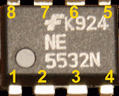
| ❏ | 4 | NE5532 Dual OpAmp |
 | DIP-8 |  | RX OpAmps | |
| ❏ | 1 | DPDT Switch | DPDT | Connects as S1A and S1B | RX OpAmps | ||
| ❏ | 1 | 10 uF/25Vdc |
 | Electrolytic | RX OpAmps | ||
| ❏ | 12 | 100 uF/25Vdc |
 | Electrolytic | RX OpAmps | ||
| ❏ | 2 | 220 uF/16Vdc |
 | Electrolytic | RX OpAmps | ||
| ❏ | 1 | 3.5mm stereo jack - PCB mount | jack | RX OpAmps | |||
| ❏ | 1 | BNC Connector Male - PCB mount | jack | RX OpAmps | |||
| ❏ | 1 | misc hookup wire | misc | RX OpAmps | |||
| ❏ | 1 | shunt wire (cut-off lead) | misc | RX OpAmps | |||
| ❏ | 4 | 10 uF (NP) |
 | Non-Polarized | RX OpAmps | ||
| ❏ | 1 | 500 (Y501) | Y501 | trimpot | RX OpAmps | ||
| ❏ | 2 | 5K (Y502) | Y502
 | trimpot | Needs to be initialized. Before installing this trimmer, adjust the resistance between the middle pin and either of the other pins to 2.5 K Ohm. | RX OpAmps |
RX OpAmps Summary Build Notes
- Install the Capacitors
- Install VK6IC Fix (optional)
- Install Resistors, etc.
- Install Ics NE5532
- Adjust Trimmer
- Install Antenna Connector
- Install RX I/Q Jack And Switch
- Install Temporary Antenna Jumper
- Test the Stage
RX OpAmps Detailed Build Notes
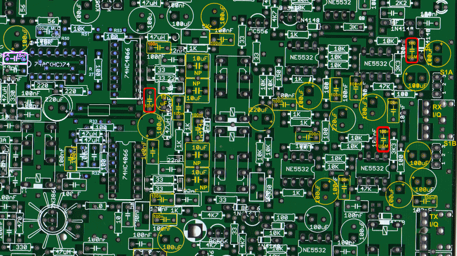
Top of the Board
Install the Capacitors
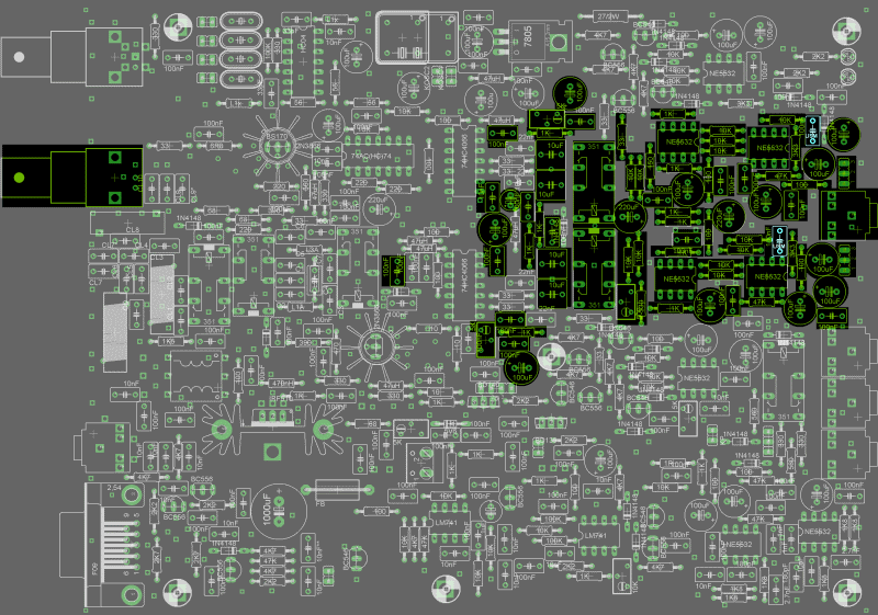
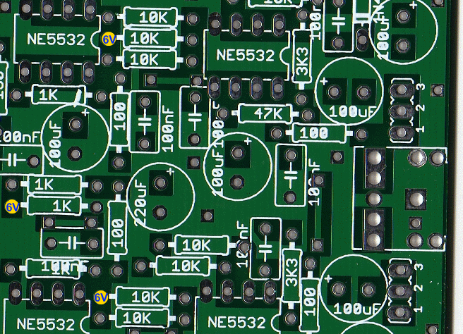
A number of capacitors, electrolytc and non-electrolytic are installed for the RX Opamp, per the graphic
| Check | Designation | Component | Marking | Category | Orientation | Notes |
|---|---|---|---|---|---|---|
| ❏ | E66 | 10 nF (.01uF) | 103
| Ceramic | ||
| ❏ | E90 | 10 uF/25Vdc |
| Electrolytic | ||
| ❏ | C3 | 100 nF | 104
| ceramic | ||
| ❏ | E120 | 100 nF | 104
| ceramic | ||
| ❏ | E155 | 100 nF | 104
| ceramic | ||
| ❏ | E170 | 100 nF | 104
| ceramic | ||
| ❏ | E172 | 100 nF | 104
| ceramic | ||
| ❏ | E248 | 100 nF | 104
| ceramic | ||
| ❏ | E258 | 100 nF | 104
| ceramic | ||
| ❏ | E26 | 100 nF | 104
| ceramic | ||
| ❏ | E268 | 100 nF | 104
| ceramic | ||
| ❏ | E343 | 100 nF | 104
| ceramic | ||
| ❏ | E43 | 100 nF | 104
| ceramic | ||
| ❏ | E72 | 100 nF | 104
| ceramic | ||
| ❏ | E74 | 100 nF | 104
| ceramic | ||
| ❏ | E76 | 100 nF | 104
| ceramic | ||
| ❏ | E80 | 100 nF | 104
| ceramic | ||
| ❏ | E114 | 10 uF (NP) |
| Non-Polarized | ||
| ❏ | E157 | 10 uF (NP) |
| Non-Polarized | ||
| ❏ | E165 | 10 uF (NP) |
| Non-Polarized | ||
| ❏ | E77 | 10 uF (NP) |
| Non-Polarized | ||
| ❏ | E129 | 100 uF/25Vdc |
| Electrolytic | ||
| ❏ | E132 | 100 uF/25Vdc |
| Electrolytic | ||
| ❏ | E151 | 100 uF/25Vdc |
| Electrolytic | ||
| ❏ | E156 | 100 uF/25Vdc |
| Electrolytic | ||
| ❏ | E207 | 100 uF/25Vdc |
| Electrolytic | ||
| ❏ | E255 | 100 uF/25Vdc |
| Electrolytic | ||
| ❏ | E259 | 100 uF/25Vdc |
| Electrolytic | ||
| ❏ | E261 | 100 uF/25Vdc |
| Electrolytic | ||
| ❏ | E275 | 100 uF/25Vdc |
| Electrolytic | ||
| ❏ | E295 | 100 uF/25Vdc |
| Electrolytic | ||
| ❏ | E71 | 100 uF/25Vdc |
| Electrolytic | ||
| ❏ | E85 | 100 uF/25Vdc |
| Electrolytic | ||
| ❏ | E127 | 100 nF USM | 104J
| Ceramic | Likely is C61 on schematic | |
| ❏ | E344 | 100 nF USM | 104J
| Ceramic | likely is C62 on schematic | |
| ❏ | E133 | 220 uF/16Vdc |
| Electrolytic | ||
| ❏ | E265 | 220 uF/16Vdc |
| Electrolytic |
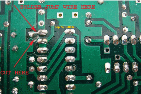
Install VK6IC Fix (optional)
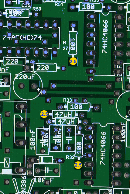
For Boards Serial Numbered from 1 to 100 (" VK6IC Fix")
Boards numbered from 1 to 100 were shipped without on or more of the modifications in the pdf file describing the fix by VK6IC. This fix calls for cutting one trace and soldering a small jumper (both in the underside of the board, in the vicinity of pins 14 and 13 of the top 74HC4066 Quad Bilteral Switch IC.
The original board design had pin 13 connected to a bypass capacitor. The modification removes that connection and makes a connection between pin 14 and the bypass capacitor. Some boards in the higher numbers of the 1-100 range have already had the trace cut but still need the jumper wire soldered, as in the case of the author's board.
| Check | Designation | Component | Marking | Category | Orientation | Notes |
|---|---|---|---|---|---|---|
| ❏ | fix | shunt wire (cut-off lead) | misc |
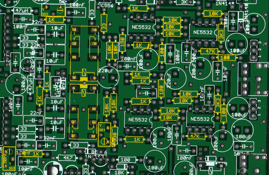
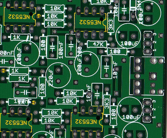
Install Resistors, etc.
Similarly, a large number of resistors, along with three pots and 2 relays, are installed for the rx opamps, per the following diagram:
| Check | Designation | Component | Marking | Category | Orientation | Notes |
|---|---|---|---|---|---|---|
| ❏ | E30 | 33 1/4W 1% | ora-ora-blk-gld-brn
| 1/4W | ||
| ❏ | E106 | 100 1/4W 1% | br-blk-blk-blk-br
| 1/4W | ||
| ❏ | E158 | 100 1/4W 1% | br-blk-blk-blk-br
| 1/4W | ||
| ❏ | E171 | 100 1/4W 1% | br-blk-blk-blk-br
| 1/4W | ||
| ❏ | E7 | 100 1/4W 1% | br-blk-blk-blk-br
| 1/4W | ||
| ❏ | E109 | 150 1/4W 1% | brn-grn-blk-blk-brn
| 1/4W | ||
| ❏ | E160 | 330 1/4W 1% | ora-ora-blk-blk-brn
| 1/4W | ||
| ❏ | E108 | 1 k 1/4W 1% | br-blk-blk-br-br
| 1/4W | ||
| ❏ | E113 | 1 k 1/4W 1% | br-blk-blk-br-br
| 1/4W | ||
| ❏ | E159 | 1 k 1/4W 1% | br-blk-blk-br-br
| 1/4W | ||
| ❏ | E163 | 1 k 1/4W 1% | br-blk-blk-br-br
| 1/4W | ||
| ❏ | E25 | 1 k 1/4W 1% | br-blk-blk-br-br
| 1/4W | ||
| ❏ | E260 | 1 k 1/4W 1% | br-blk-blk-br-br
| 1/4W | ||
| ❏ | E264 | 1 k 1/4W 1% | br-blk-blk-br-br
| 1/4W | ||
| ❏ | E61 | 1 k 1/4W 1% | br-blk-blk-br-br
| 1/4W | ||
| ❏ | E63 | 1 k 1/4W 1% | br-blk-blk-br-br
| 1/4W | ||
| ❏ | E67 | 1 k 1/4W 1% | br-blk-blk-br-br
| 1/4W | ||
| ❏ | E135 | 3k3 1/4W 1% (3.3K) | ora-ora-blk-brn-brn
| 1/4W | ||
| ❏ | E257 | 3k3 1/4W 1% (3.3K) | ora-ora-blk-brn-brn
| 1/4W | ||
| ❏ | E110 | 10 k 1/4W 1% | br-blk-blk-r-br
| 1/4W | ||
| ❏ | E112 | 10 k 1/4W 1% | br-blk-blk-r-br
| 1/4W | ||
| ❏ | E115 | 10 k 1/4W 1% | br-blk-blk-r-br
| 1/4W | ||
| ❏ | E116 | 10 k 1/4W 1% | br-blk-blk-r-br
| 1/4W | ||
| ❏ | E117 | 10 k 1/4W 1% | br-blk-blk-r-br
| 1/4W | ||
| ❏ | E118 | 10 k 1/4W 1% | br-blk-blk-r-br
| 1/4W | ||
| ❏ | E161 | 10 k 1/4W 1% | br-blk-blk-r-br
| 1/4W | ||
| ❏ | E162 | 10 k 1/4W 1% | br-blk-blk-r-br
| 1/4W | ||
| ❏ | E166 | 10 k 1/4W 1% | br-blk-blk-r-br
| 1/4W | ||
| ❏ | E167 | 10 k 1/4W 1% | br-blk-blk-r-br
| 1/4W | ||
| ❏ | E168 | 10 k 1/4W 1% | br-blk-blk-r-br
| 1/4W | ||
| ❏ | E169 | 10 k 1/4W 1% | br-blk-blk-r-br
| 1/4W | ||
| ❏ | E136 | 47K 1/4W 1% | yel-vio-blk-red-brn
| 1/4W | ||
| ❏ | E256 | 47K 1/4W 1% | yel-vio-blk-red-brn
| 1/4W | ||
| ❏ | E10 | JRC27F/012 relay | JRC27F/012 | 12V relay | ||
| ❏ | E9 | JRC27F/012 relay | JRC27F/012 | 12V relay | ||
| ❏ | E296 | 500 (Y501) | Y501 | trimpot | ||
| ❏ | E17 | 5K (Y502) | Y502
| trimpot | Needs to be initialized. Before installing this trimmer, adjust the resistance between the middle pin and either of the other pins to 2.5 K Ohm. | |
| ❏ | E18 | 5K (Y502) | Y502
| trimpot | Needs to be initialized. Before installing this trimmer, adjust the resistance between the middle pin and either of the other pins to 2.5 K Ohm. |
Install Ics NE5532
The four NE5532s that provide the RX OpAmp chain are installed as the center two chains of an array of four chains of NE5532s. The builder needs to take care to install in the RX opamps' holes, not the TX opamps's holes. The builder must also pay close attention to the orientation of the opamps. They are installed such that their printing is upside down, with the marking dot oriented "top right".
Some have asked whether they could/should use sockets. The answer has been "It is OK to use sockets for these ICs, but the sockets must be of the highest quality" (a large cost issue).
If the builder is NOT using sockets, follow the maxim "Measure twice, cut once", since these brutes are hard to get out once soldered in.
| Check | Designation | Component | Marking | Category | Orientation | Notes |
|---|---|---|---|---|---|---|
| ❏ | E153 | NE5532 Dual OpAmp |
| DIP-8 | | Take ESD precautions |
| ❏ | E154 | NE5532 Dual OpAmp |
| DIP-8 | | Take ESD precautions |
| ❏ | E69 | NE5532 Dual OpAmp |
| DIP-8 | | Take ESD precautions |
| ❏ | E70 | NE5532 Dual OpAmp |
| DIP-8 | | Take ESD precautions |
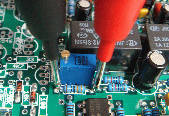
Adjust Trimmer
With the power OFF, adjust trimpot Y501 until the resistance across the 300 ohm resistor is 150 ohms.
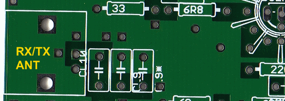
Install Antenna Connector
Install the bnc jack on the left-hand edge of the board
| Check | Designation | Component | Marking | Category | Orientation | Notes |
|---|---|---|---|---|---|---|
| ❏ | E137 | BNC Connector Male - PCB mount | jack |
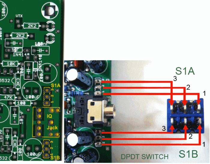
Install RX I/Q Jack And Switch
-
RX I/Q Audio Jack
Mount the stereo jack on the right-hand side of the board per the graphic. -
Additional Op-Amp Switches, S1a and S1b
Then, connect the DPDT Switch S1 to the two 3-pin points on the right-hand side of the board, such that each of the wires for each of the (A and B) of pins on S1 line up: "1" on the switch with "1" on the board, "2" with "2" , etc.
These switches allow you to add another op-amp stage to the RX chain, boostongf the gain from 23dB to 46dB.
| Check | Designation | Component | Marking | Category | Orientation | Notes |
|---|---|---|---|---|---|---|
| ❏ | E141 | DPDT Switch | DPDT | Connects as S1A and S1B | ||
| ❏ | E137 | 3.5mm stereo jack - PCB mount | jack |
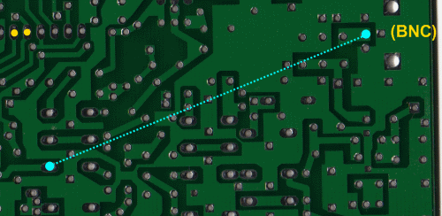
Install Temporary Antenna Jumper
"Tack" solder a wire to connect the antenna "hot" pin on the BNC connector to the Mixer Stage's Input point on the board
The wire connects the antenna "hot" terminal in the BNC connector to the point where a not-yet-installed relay will switch the antenna in/out of the TX /RX path(s). Soldering to the BNC is simple; soldering to the relay pin should be done carefully so as to "tack" the wire to the hole's surrounding pad, yet NOT fill the hole up with solder, thus, making the subsequent installation of the relay considerably easier.
| Check | Designation | Component | Marking | Category | Orientation | Notes |
|---|---|---|---|---|---|---|
| ❏ | wire5 | misc hookup wire | misc |
RX OpAmps Testing
Current Draw
Test Setup
Check RX current consumption - it should low, around 120 mA.
Much higher current readng will indicate leakage to ground
Very low current usually means no connection (e.g., a blown diode somewhere in the circuit).
Voltage Tests - 6V
Test Setup
Power up the board
Measure the voltages on each of the NE5532 OpAmps. Each OpAmp's voltages must be the same for each corresponding pin (see the table below)
When all OpAmps are working correctly, the +voltage is determined by your input voltage. Typically the voltage at pins 1-3 and 5-7 is around +6 to 6.5V with +13.8Vin and around +5.5V with +12Vin.
The exact voltage on the NE5532 (pins 1-3 and 5-7) is not critical at all. Any value around +6V is just fine. However what really matter is that the voltage on all pins of all four NE552s is identical or at least symmetrical.
This information is important for us for two practical reasons:
- Firstly, it tells us whether all the resistors around the OpAmps have been installed correctly.
- Secondly, it tells us if all the NE OpAmpss are working properly- otherwise proper I / Q shift adjustment may not be possible.
Test Measurements
| Testpoint | Units | Nominal Value | Author's | Yours |
|---|---|---|---|---|
| All NE5532: Pins 1, 2, 3, 5, 6, 7 | V dc | 6.0 | 5.9 (Vcc=12.6) | _______ |
| All NE5532: Pin 4 | V dc | 0 | 0 | _______ |
| All NE5532: Pin 8 | V dc | 12 | 11.2 (Vcc=12.6) | _______ |
2.5V dc Tests
Test Setup
With power on, measure the voltage at the "+2.5" testpoints (white circles). The voltage should be approximately 50% of the 5 V rail voltage
Test Measurements
| Testpoint | Units | Nominal Value | Author's | Yours |
|---|---|---|---|---|
| Point 2 | Vdc | 2.5 | 2.45 | _______ |
| Point 1 | Vdc | 2.5 | 2.49 | _______ |
Mixer Pin Voltages
Test Setup
With power on, measure the voltage at the designated pins (see table below) of each mixer IC (74HC4066).
Test Measurements
| Testpoint | Units | Nominal Value | Author's | Yours |
|---|---|---|---|---|
| Pin 5 | V dc | 2.5 | 2.49 | _______ |
| Pin 6 | V dc | 2.5 | 2.49 | _______ |
| Pin 12 | V dc | 2.5 | 2.49 | _______ |
| Pin 13 | V dc | 2.5 | 2.49 | _______ |
| Pin 14 | V dc | 5 | 5.02 | _______ |
RX Testing - Image Adjustment
Test Setup
Connect an antenna to the BNC antenna jack on the G40
Connect the G40 to your PC using plug cables between the RX I/Q jack and the PC's Stereo Line-In input (or MIC input, if the PC has a stereo MIC input).
Start your SDR program of choice and set the center frequency at 7.047 MHz (you may want to use the GSDR program - Hans LA2MOA's setup instructions are here.
Power on the G40.
You should see some 40m signals if your RX is working. See the video of :Bojan S51QA's test at this point.
Image Rejection Adjustment
It is crucial that after the build phase 5 image rejection is adjusted properly.
"Images" are a common artifact of the Direct Conversion receiver which is the basis for this SDR. They are encountered in the display when:
- the phasing of the I and Q signals is not just right; OR
- when only one of the two signals is present, either because of a bad connection or a mono soundcard input.
Images are pretty obvious on the spectrum display of the SDR, looking like mirror inage signals on either side of the center frequency. One of these is the desired signal; the other is an image that should be rejected. For example, if the center frequency is 7.047 MHz and your desired signal is 7.057 MHz (10 kHz above the center "zero"), then there may be a mirror image of that signal at 7.037 MHz (10 kHz below the center "zero"). Adjusting for image rejection causes these unwanted images to disappear down into the noise level.
To begin, Download and setup Winrad to serve as a SDR receiving program
Image adjustment will require a running SDR program tuned to 7.047 Images are eliminated by properly adjusting the hardware, using the
techniques described on the G40 website.
Follow these techniques to correctly adjust your receiver.
(See also the excellent Video by Josh VK2FJDX (fast forward to minute 4:40). If you don't understand that, you need help!)