Final Tests and Adjustments Introduction
General
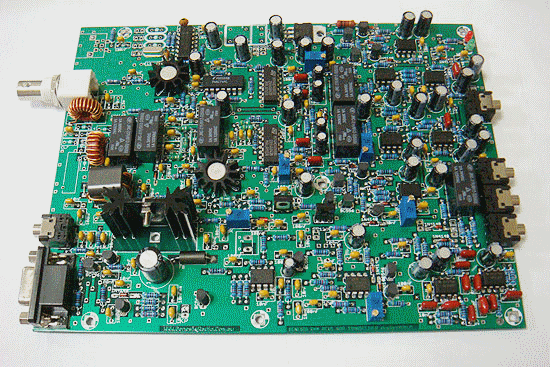
This stage contains the final adjustments and tests needed to get your G40 on the air!
Final Tests and Adjustments Bill of Materials
Final Tests and Adjustments Summary Build Notes
- Install Final, Permanent Wires
- Test the Stage
Final Tests and Adjustments Detailed Build Notes
Top of the Board
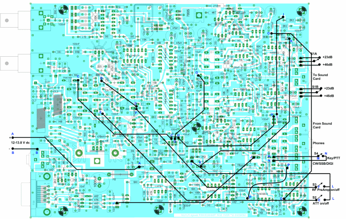
Install Final, Permanent Wires
In this final stage, we police up the various wire connections that represent the final board configuration. We remove any temporary wires and validate that all permanent wires and switches are correctly installed. Then we commence the final series of tests.
(Click here for a high-resolution image of the final wires layout)
And click here for a high-resolution image of wiresw and switches, combined.
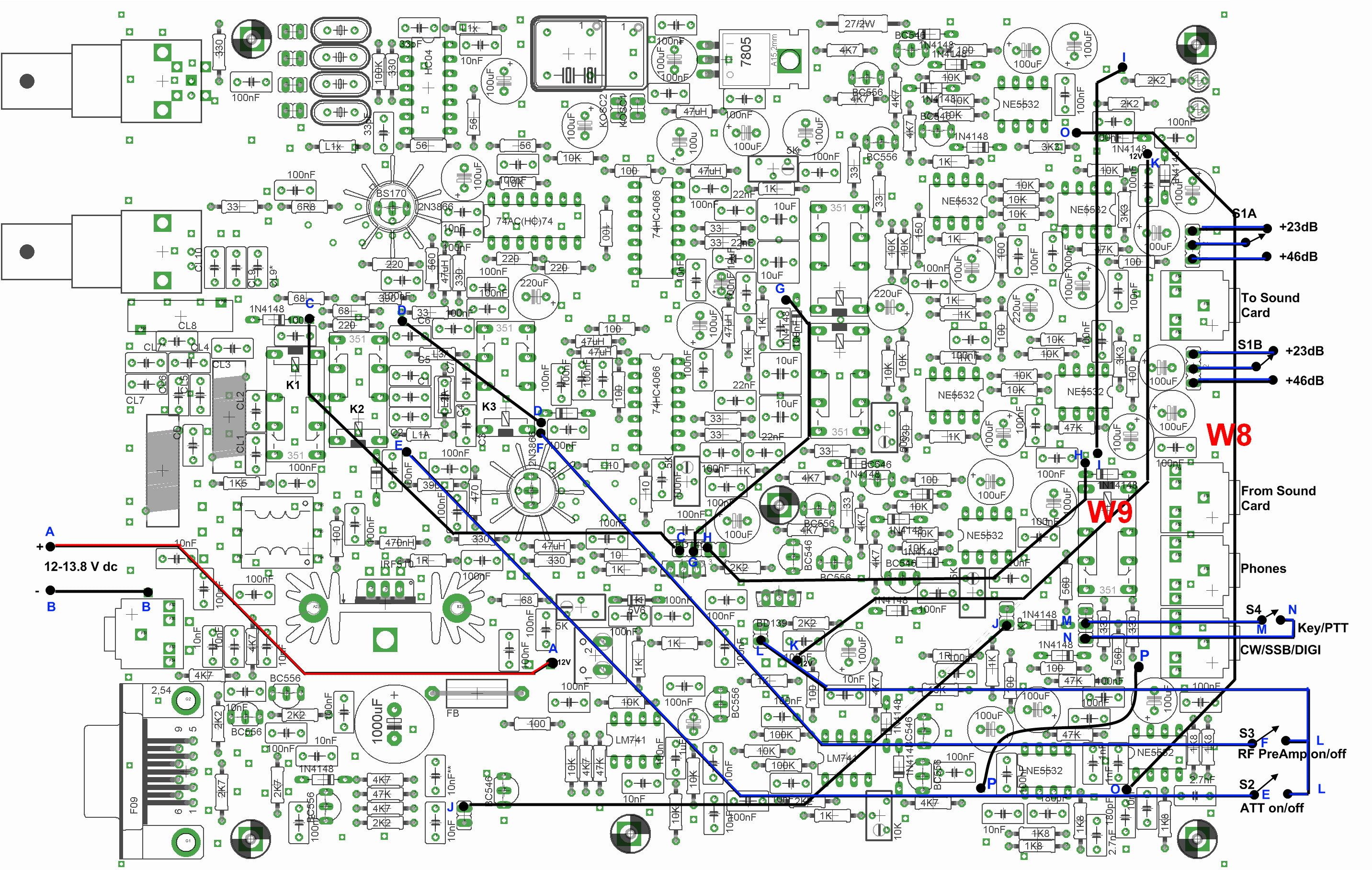
Final Tests and Adjustments Testing
Test OpAmp Pin Voltages
Test Setup
When we say in the following tests that "the voltage must be identical" we expect the builder to see a very close value on all pins, but NOT absolutely identical voltage. We are really looking for mismatch of lets say +/- 1V or so, which would be an indication of incorrectly placed component (most likely a resistor, diode or transistor) or faulty op amp. Because individual components used have their own tolerance, slight deviation is quite normal, expected and acceptable.
Before you can check voltage on NE5532's in this, ensure you connected the permanent wires specified at the end of Phase 6. Those wires supply + voltage to the four TX NE5532 installed above. Basically make sure that you have +12 to 13V on pin 8 on all NE5532.
This series of tests applies equally to each of the four RX and four TX NE5532s.
- Apply power to the board.
- Check out voltage on each of the 8 ICs NE5532
- Note that the RX ICs are installed with their "1" pins at the upper right of each chip; the TX ICs are installed with the "1" pin at the lower left of each IC.
- pins 1,2,3,5,6,7. [+5.70V to + 6.00V]
- This voltage must be essentially identical on all of the specified pins for all eight ICs.
| Pin | IC-A | IC-B | IC-C | IC-D | IC-E | IC-F | IC-G | IC-H |
|---|---|---|---|---|---|---|---|---|
| 1 | 5.91 | 5.84 | 5.84 | 5.85 | 5.85 | 5.84 | 5.84 | 5.82 |
| 2 | 5.85 | 5.84 | 5.84 | 5.84 | 5.84 | 5.84 | 5.83 | 5.82 |
| 3 | 5.85 | 5.84 | 5.84 | 5.84 | 5.84 | 5.84 | 5.83 | 5.82 |
| 4 | 0 | 0 | 0 | 0 | 0 | 0 | 0 | 0 |
| 5 | 5.85 | 5.85 | 5.84 | 5.85 | 5.84 | 5.84 | 5.80 | 5.79 |
| 6 | 5.85 | 5.85 | 5.84 | 5.85 | 5.84 | 5.84 | 5.83 | 5.82 |
| 7 | 5.79 | 5.87 | 5.84 | 5.86 | 5.84 | 5.84 | 5.83 | 5.82 |
| 6 | 10.99 | 11.03 | 11.03 | 11.03 | 11.04 | 11.04 | 11.8 | 11.8 |
Additional Voltage Tests
Test Setup
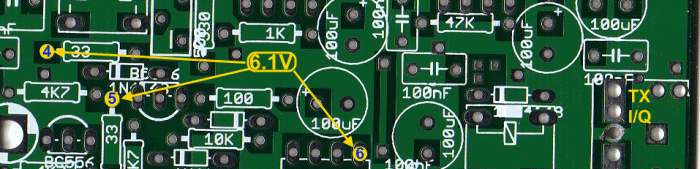
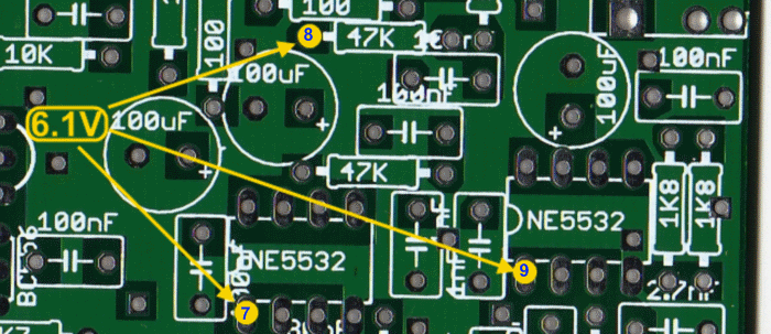
Measure the dc voltage at each of the testpoints shown in the following graphics. Each test point should have the same voltage (it will be in the range of 6.0-6.1 Vdc, but whatever the value, it should be the same at each testpoint)
Upper Right Test Points
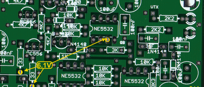
Middle Area Testpoints
Lower Right Test Points
Test Measurements
| Testpoint | Units | Nominal Value | Author's | Yours |
|---|---|---|---|---|
| Point 1 | V dc | 6.1 | 5.75 | _______ |
| Point 2 | V dc | 6.1 | 5.87 | _______ |
| Point 3 | V dc | 6.1 | 5.81 | _______ |
| Point 4 | V dc | 6.1 | 5.74 | _______ |
| Point 5 | V dc | 6.1 | 5.88 | _______ |
| Point 6 | V dc | 6.1 | 5.80 | _______ |
| Point 7 | V dc | 6.1 | 5.78 | _______ |
| Point 8 | V dc | 6.1 | 5.81 | _______ |
| Point 9 | V dc | 6.1 | 5.79 | _______ |
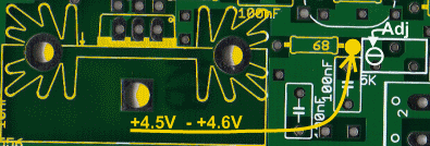
Voltage Test
Test Setup
Power ON
Power up the SDR Software (e.g., GSDR) and put the rig into TX mode (e.g., using the "TUN" button)
Test the voltage at the testpoint.
You should see between 4.5 and 4.6 V dc
Return the rig to RX mode/remove power from the rig
Final RX/TX Test
Test Setup
Adjust the quiescent current at FET gate voltage to +4.5-+4.6V (as in above voltage test).
Connect the SDR transceiver to a good resonant antenna or a 50 Ohm dummy load.
Initial adjustment: you would need a separate ‘control’ receiver tuned on the 40m band.
Normally, the carrier will be fully balanced out at near, but not exactly 2.50 volts each, and they may be not quite exactly the same (maybe a few hundredths of volts different) when the carrier just disappears below the noise in control receiver (way below S0). That is what you want, not matched voltages on a voltmeter. I also think, without going back to check, that you can get this null at many voltage points near 2.5, and any of them will be fine, so long as they null out the carrier near the 2.50 point. So, do not chase the same voltage from one trimmer to the other. Seek the null. Tx to Preston WJ2V for this tip.
- Disconnect the soundcard input [TX I/Q “From sound card jack”]
- Tune the control receiver to 7046 KHz
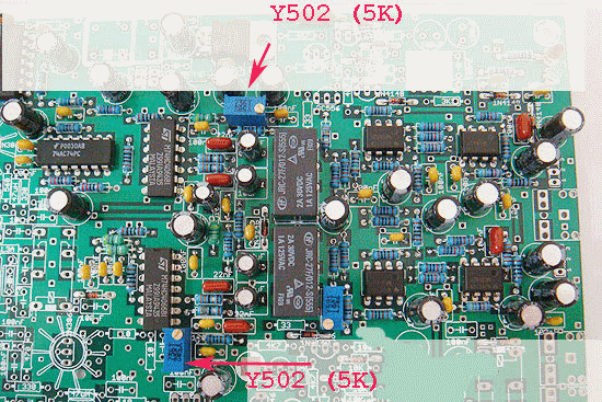
- Adjust the 5K trimmers for minimum signal strength (typical voltage at trimmer is +2.5V +/- 0.1-0.2V) Both of the 502 pots must match for Transmit I and Q carrier null to work properly. They should be set to exactly 2.50 volts wiper-to-ground. The two 502 pots that will null your carrier within a few hundreths of a volt from each other and very close to 2.50 volts.
- Connect the sound card TX I/Q output to the "From PC Soundcard" jack
- On the control RX, adjust the max image rejection with the G40's 5K trimmer.

- Tune the G40 to 7.037 MHz and transmit into your dummy load
- set your 'big radio' receiver to image freq. of 7.057 MHz
- adjust trimmer pot while observing image signal strength on receiver's S meter. Typically image sig should drop from S6 to S1.
[Please note: refer to G40 homepage for more information in regard to adjustment procedure and Connection to Sound card and PC.]
To test the completed G40 Transceiver, the builder is directed to the extensively documented RX/TX Test Procedure on the GenesisRadio website.