Transmitter PA Introduction
General
This stage provides the Class A PA based on Mitsubishi RF MOSFET RD16HHF1.
It is always a good idea to double check the bill of materials in this set of documentation with the official BOM on the Mobo site. Discrepancies may be introduced inadvertently, as the changes are sometimes not communicated or discovered, making timely update of this site a problem.
Theory of Operation
When biased to Class A (the biasing is done via software control and user customisable), a very linear output for SSB and digital modes is possible. When driven hard (beyond CLASS A limits), the linearity will decline. Measured IMD Ratios (a measure of the whole Tx chain's linearity) on the ALPHA build are:>/p>
- 1WPEP 48dBIMDR(tone to IMD level)
- 2WPEP 46dBIMDR
- 4WPEP 37dBIMDR
- 5WPEP 31dBIMDR
- 6WPEP 27dBIMDR
- 7WPEP 23dBIMDR
Transmitter PA Schematic
(Click for Full Schematic)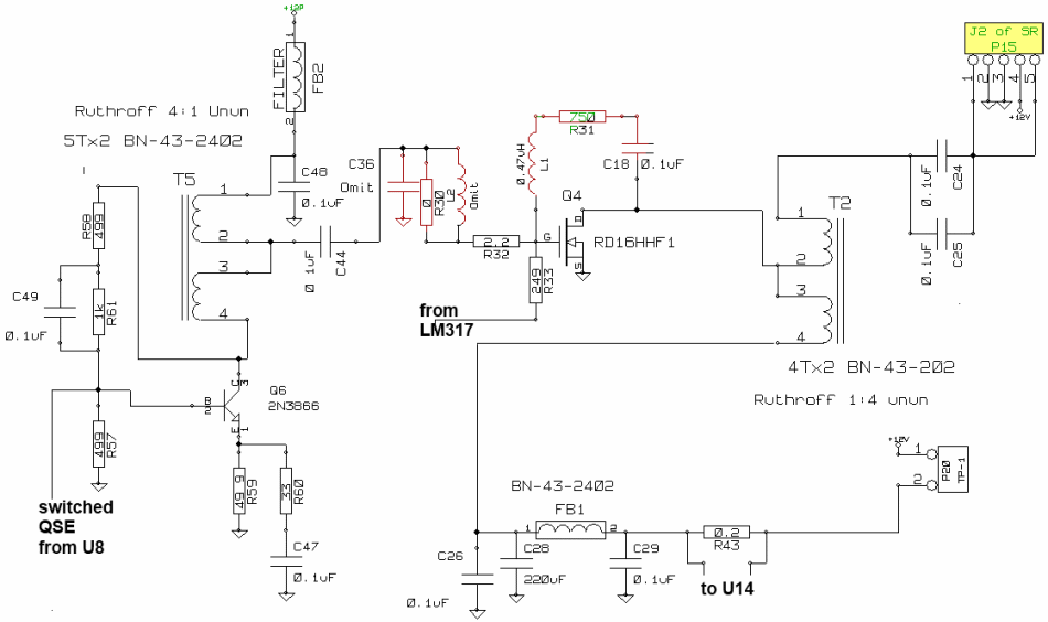
C:\Users\Rob\Documents\HamStuff\SDR\MOBO4_x\mobo43
(above schematic has clickable areas that can be used for navigation)
(go directly to build notes)Transmitter PA Bill of Materials
Stage Bill of Materials
(resistor images and color codes courtesy of WIlfried, DL5SWB's R-Color Code program)
| Check | Count | Component | Marking | Category |
|---|---|---|---|---|
| ❏ | 1 | BN43-202 |
 | Binocular core |
| ❏ | 1 | BN-43-2402 (no markings!) | none
| Binocular core |
| ❏ | 1 | BN-43-2402 (no markings!) | none
| Binocular core |
| ❏ | 1 | 220 uF/16Vdc |
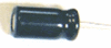 | Electrolytic |
| ❏ | 1 | header, 2-pin |
 | Header |
| ❏ | 1 | TO-220 heatskink | Misc | |
| ❏ | 1 | shunt, 2-pin |
 | Shunt |
| ❏ | 1 | FERRITE CHIP 120 OHM 500MA 0805 |
 | SMT |
| ❏ | 4 | 0.1 uF | SMT 0805 | |
| ❏ | 1 | 0.1 uF | SMT 0805 | |
| ❏ | 1 | 0 ohm 5% | SMT 0805 1/8W | |
| ❏ | 1 | 1 k ohm 1% | SMT 0805 1/8W | |
| ❏ | 1 | 2.2 ohm 1% | SMT 0805 1/8W | |
| ❏ | 1 | 249 ohm 1% | SMT 0805 1/8W | |
| ❏ | 1 | 33 ohm 1% | SMT 0805 1/8W | |
| ❏ | 1 | 49.9 ohm 1% | SMT 0805 1/8W | |
| ❏ | 2 | 499 ohm 1% | SMT 0805 1/8W | |
| ❏ | 1 | 750 ohm 1% | SMT 0805 1/8W | |
| ❏ | 2 | 0.1 uF | (smt) black stripe
 | SMT 1206 |
| ❏ | 1 | 0.2 ohm 5% | SMT 1206 1/4W | |
| ❏ | 1 | 0.47 uH 20% | SMT 1210 | |
| ❏ | 1 | ZXCT1021 low sense voltage monitor | ZXCT1021
 | SOT-23-5 |
| ❏ | 1 | RD16HHF1 MOSFET RF OUTPUT TRANSISTOR | RD16HHF1
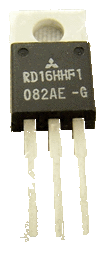 | TO-220 |
| ❏ | 1 | 2N3866 NPN Transistor |
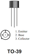 | TO-39 |
Transmitter PA Summary Build Notes
- Install Bottomside Rs and Cs
- Install U14
- Install Topside Rs, Cs, and Ferrite
- Wind and Install Inductors
- Install Connectors
- Install Transistors and Heatsinks
- Test the Stage
Transmitter PA Detailed Build Notes
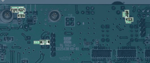
Bottom of the Board
Install Bottomside Rs and Cs
| Check | Designation | Component | Marking | Category | Orientation | Notes |
|---|---|---|---|---|---|---|
| ❏ | C47 | 0.1 uF | SMT 0805 | |||
| ❏ | R30 | 0 ohm 5% | SMT 0805 1/8W | |||
| ❏ | R32 | 2.2 ohm 1% | SMT 0805 1/8W | |||
| ❏ | R43 | 0.2 ohm 5% | SMT 1206 1/4W | |||
| ❏ | R59 | 49.9 ohm 1% | SMT 0805 1/8W | |||
| ❏ | R33 | 249 ohm 1% | SMT 0805 1/8W |
Top of the Board
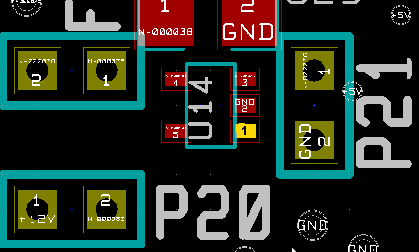
Install U14
U14 - the voltage monitor - would normally be associated electronically with the next phase. However, due to the close quarters around this tiny IC, it is installed during this phase. Take great care to avoid solder bridges, since, once this phase is completed, getting access to the IC will be quite difficult.
| Check | Designation | Component | Marking | Category | Orientation | Notes |
|---|---|---|---|---|---|---|
| ❏ | U14 | ZXCT1021 low sense voltage monitor | ZXCT1021
| SOT-23-5 | Take ESD precautions |
Install Topside Rs, Cs, and Ferrite
FB2 is an SMT RF choke - no winding required :>}. The parts supplied include an extra BN43-2402 for those who would prefer to wind this choke: 6T #30 for 56uH.
| Check | Designation | Component | Marking | Category | Orientation | Notes |
|---|---|---|---|---|---|---|
| ❏ | FB2 | FERRITE CHIP 120 OHM 500MA 0805 |
| SMT | SMT (optional:6T (8") #30 on BN43-2402 for 56uH) | |
| ❏ | C18 | 0.1 uF | SMT 0805 | |||
| ❏ | C26 | 0.1 uF | (smt) black stripe
| SMT 1206 | ||
| ❏ | C48 | 0.1 uF | SMT 0805 | Install C48 before installing C28 | ||
| ❏ | C29 | 0.1 uF | (smt) black stripe
| SMT 1206 | ||
| ❏ | C44 | 0.1 uF | SMT 0805 | |||
| ❏ | C49 | 0.1 uF | SMT 0805 | |||
| ❏ | R31 | 750 ohm 1% | SMT 0805 1/8W | |||
| ❏ | R57 | 499 ohm 1% | SMT 0805 1/8W | |||
| ❏ | R58 | 499 ohm 1% | SMT 0805 1/8W | |||
| ❏ | R60 | 33 ohm 1% | SMT 0805 1/8W | |||
| ❏ | R61 | 1 k ohm 1% | SMT 0805 1/8W | |||
| ❏ | L01 | 0.47 uH 20% | SMT 1210 | |||
| ❏ | C28 | 220 uF/16Vdc |
| Electrolytic |
Wind and Install Inductors
Wind and install the transformers and chokes (refer to the preceding stage for transformer winding instructions).
Transformers
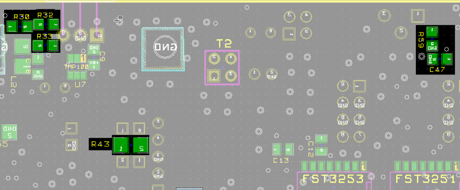
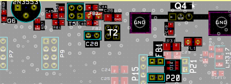
T2
T2 is wound on the larger BN43-202, using 4 turns of a a bifilar length (16" total) of #26 (or heavier) wire.
Note that T2 is erroneously shown on the PCB as being installed to the bottom (Cu) side; this is an error. T2 must be installed to the top (Cmp) side in the 4 holes provided.
Use a continuity checker to separate out the 2 pairs of windings. One winding goes to the left 2 holes, and the other winding goes to the right 2 holes. This way, the flat surfaces of the BN core faces east-west.
T5
T5 is wound on a BN43-2402 binocular core using 5 turns of a bifilar length of #30 wire (11" total wire length)
One winding goes to the left two holes and one winding goes to the right 2 holes.
The core is oriented so that its two holes are in a vertical (north-south) row.
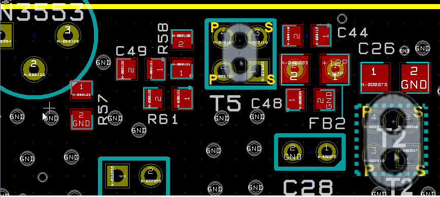
Choke
FB1 is wound on a BN 43-2402 binocular core with a 4 inch length #26 (or thicker) magnet wire. The number of turns Is 3. The inductance (for turns verification purposes only) should be about 11.7 uH
Install Connectors
| Check | Designation | Component | Marking | Category | Orientation | Notes |
|---|---|---|---|---|---|---|
| ❏ | P20 | header, 2-pin |
| Header | TP1 - Drain Current Test Point 1 Jumper 1-2 for normal Op. Unjumper to measure drain current with external Ammeter | |
| ❏ | P20_Shunt | shunt, 2-pin |
| Shunt | Install shunt for normal operation; remove to measure drain current |
Install Transistors and Heatsinks
In mounting the large heatsink, use only the nylon spacer for the pcb bottom on the side closer to the USB connector. This is to avoid shorting to the nearby traces. On the other side and for the pcb top, try to replace the nylon spacers with metal spacers. We recommended putting a "star" metal spacer because it conducts RF but has fair thermal isolation. Therefore you will have good RF grounding of the heatsink via 3 of the pcb surfaces.
Make sure that the Heatsink has a good ground to the Mobo PCB through the mounting screws, preferably using a locking washer. If the Heatsink is not grounded, you WILL get VHF oscillation in the PA.
| Check | Designation | Component | Marking | Category | Orientation | Notes |
|---|---|---|---|---|---|---|
| ❏ | Q06 | 2N3866 NPN Transistor |
| TO-39 | ||
| ❏ | Q04 | RD16HHF1 MOSFET RF OUTPUT TRANSISTOR | RD16HHF1
| TO-220 | Take ESD precautions | |
| ❏ | Q04_heatsink | TO-220 heatskink | Misc | Heatsink mounting hardware to be supplied by kit buyer. Suggested that external star washers in conjunction with metallic flat washers be used.
Heatsink must be at ground potential for best amplifier stability. |
Transmitter PA Completed Stage
Top of the Board
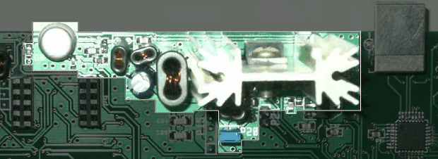
Bottom of the Board