Local Oscillators Introduction
General
This phase provides the local oscillator functionality, ultimately yielding four different center frequencies, one for the 30m band and three for the 20m band:
- 30m: 10.125 MHz
- 20m: 14.045 MHz
- 20m: 14.138 MHz
- 20m: 14.232 MHz
The Local Oscillator stage produces 4 crystal-controlled frequencies, each of which is 4 times the desired center frequency (those LO frequencies will be divided by 4 in a follow-on stage to get to the desired center frequencies.
The center frequencies provide a bandwith of either +- 24 kHZ or +- 48 kHz, depending upon the soundcard's sampling frequency of 48kHz or 96 kHz:
| Crystal | 48kHz Bandwidth | 96kHz Bandwidth |
|---|---|---|
| (40.5 MHz) 30m: center = 10.125 MHz | 10.101MHz - 10.149MHz | 10.077MHz - 10.173MHz |
| (56.180 MHz) 20m: center=14.045 MHz | 14.021MHz - 14.069MHz | 13.997MHz - 14.093MHz |
| (56.552 MHz) 20m: center = 14.138 MHz | 14.114MHz - 14.162MHz | 14.090MHz - 14.186MHz |
| (56.928 MHz) 20m: center = 14.232 MHz | 14.208MHz - 14.256MHz | 14.184MHz - 14.280MHz |
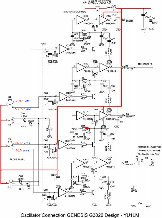
The local oscillator stage generates signals (for quadrature clocking signals of 1/4 of the selected output frequency) using a 74HC04 hex inverter and a freequency-specific crystals.
The circuit is described in more detail in the schematic "Oscillator Connection Genesis G** Design" (including the facility to bypass the internal oscillator and use, in its stead, an external oscillator).
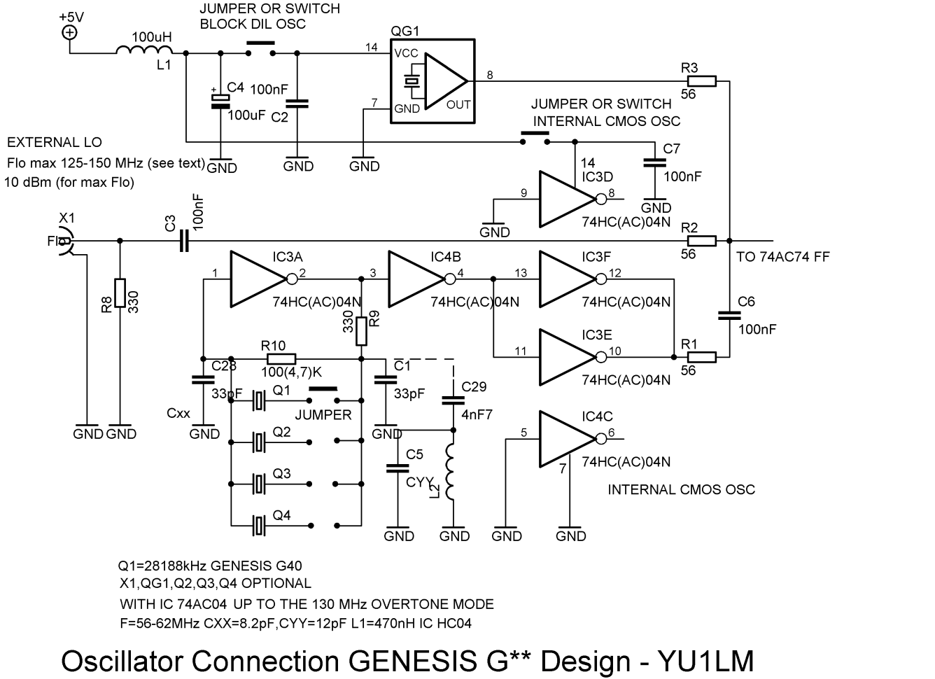
The output of this stage will divided in the follow-on stage.
(go directly to build notes)Local Oscillators Schematic
(go directly to build notes)
Local Oscillators Bill of Materials
Stage Bill of Materials
(resistor images and color codes courtesy of WIlfried, DL5SWB's R-Color Code program)
| Check | Count | Component | Marking | Category |
|---|---|---|---|---|
| ❏ | 4 | 100k 1/4W 1% | brn-blk-blk-orng-brn
 | 1/4W |
| ❏ | 6 | 10K 1/4W 1% | brn-blk-blk-red-brn
 | 1/4W |
| ❏ | 5 | 330 1/4W 1% | ora-ora-blk-blk-brn
 | 1/4W |
| ❏ | 4 | 4K7 1/4W 1% (4.7K) | yel-vio-blk-brn-brn
 | 1/4W |
| ❏ | 4 | 1N4148 | 1N4148
 | Axial |
| ❏ | 6 | 10 nF (.01uF) | 103
 | Ceramic |
| ❏ | 6 | 100 nF | 104
 | Ceramic |
| ❏ | 4 | 470 nH molded inductor (0.47 uH) | yel-vio-slv_gld
 | Choke |
| ❏ | 2 | 74HC04 Hex Inverter |
 | DIP-14 |
| ❏ | 4 | 12 pF disc ceramic | 12J
 | Disc |
| ❏ | 3 | 15 pF disc ceramic | 15J
 | Disc |
| ❏ | 1 | 22 pF disc ceramic | 22J
 | Disc |
| ❏ | 1 | 100 uF/25Vdc |
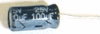 | Electrolytic |
| ❏ | 4 | BC546 NPN Transistor |
| TO-92 |
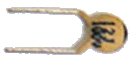
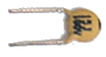
| ❏ | 1 | 40.500 MHz HC48S Crystal |
 | Xtal |
| ❏ | 1 | 56.180 MHz HC48S Crystal |
| Xtal |
| ❏ | 1 | 56.552 MHz HC48S Crystal |
| Xtal |
| ❏ | 1 | 56.928 MHz HC48S Crystal |
| Xtal |
Local Oscillators Summary Build Notes
- Install Diodes
- Install the Passive Components
- Install Active Components
- Inspect Completed Board
- Test the Stage
Local Oscillators Detailed Build Notes
Top of the Board
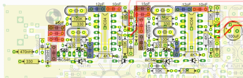
Install Diodes
Watch out on the diodes; one of them (D2-2) has its orientation (its band orientation) different from the other three
There are also 4 chokes (note they are all 470 nH (nano), NOT 47 uH (micro)). Check the color codes.
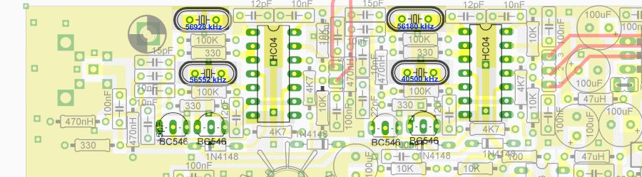
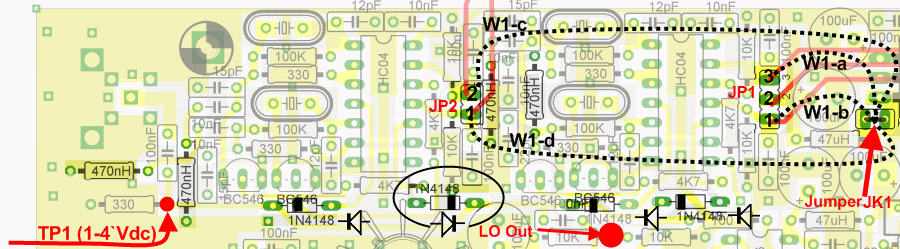
Note: The wires shown as black dotted lines on the graphic below illustrate the 4 possible, temporary connections (to the 5V present at the noted Jumper) needed to enable one of the 4 crystals. Ignore these until the testing section.
| Check | Designation | Component | Marking | Category | Orientation | Notes |
|---|---|---|---|---|---|---|
| ❏ | D2-1 | 1N4148 | 1N4148
| Axial | Band on left | |
| ❏ | D2-2 | 1N4148 | 1N4148
| Axial | Band on right | |
| ❏ | D2-3 | 1N4148 | 1N4148
| Axial | Band on left | |
| ❏ | D2-4 | 1N4148 | 1N4148
| Axial | Band on left | |
| ❏ | L2-1 | 470 nH molded inductor (0.47 uH) | yel-vio-slv_gld
| Choke | ||
| ❏ | L2-2 | 470 nH molded inductor (0.47 uH) | yel-vio-slv_gld
| Choke | ||
| ❏ | L2-3 | 470 nH molded inductor (0.47 uH) | yel-vio-slv_gld
| Choke | ||
| ❏ | L2-4 | 470 nH molded inductor (0.47 uH) | yel-vio-slv_gld
| Choke |
Install the Passive Components
Watch out for those square pass-through holes
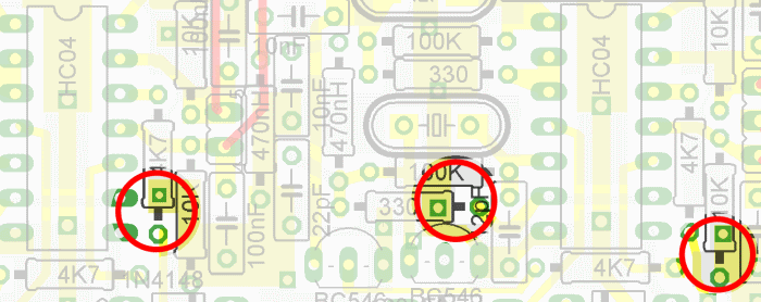
For example, in the above image, there are three different resistors where the builder can accidentally install the resistor into the round hole on one end and the square hole on the other; the holes should be round for the correct installation.
| Check | Designation | Component | Marking | Category | Orientation | Notes |
|---|---|---|---|---|---|---|
| ❏ | C2-21 | 100 uF/25Vdc |
| Electrolytic | "+" (longer lead) is on left | (reloc) |
| ❏ | R2-1 | 330 1/4W 1% | ora-ora-blk-blk-brn
| 1/4W | ||
| ❏ | R2-2 | 330 1/4W 1% | ora-ora-blk-blk-brn
| 1/4W | ||
| ❏ | R2-3 | 330 1/4W 1% | ora-ora-blk-blk-brn
| 1/4W | ||
| ❏ | R2-4 | 330 1/4W 1% | ora-ora-blk-blk-brn
| 1/4W | ||
| ❏ | R2-5 | 330 1/4W 1% | ora-ora-blk-blk-brn
| 1/4W | ||
| ❏ | R2-6 | 4K7 1/4W 1% (4.7K) | yel-vio-blk-brn-brn
| 1/4W | ||
| ❏ | R2-7 | 4K7 1/4W 1% (4.7K) | yel-vio-blk-brn-brn
| 1/4W | ||
| ❏ | R2-8 | 4K7 1/4W 1% (4.7K) | yel-vio-blk-brn-brn
| 1/4W | ||
| ❏ | R2-9 | 4K7 1/4W 1% (4.7K) | yel-vio-blk-brn-brn
| 1/4W | ||
| ❏ | R2-10 | 10K 1/4W 1% | brn-blk-blk-red-brn
| 1/4W | ||
| ❏ | R2-11 | 10K 1/4W 1% | brn-blk-blk-red-brn
| 1/4W | ||
| ❏ | R2-12 | 10K 1/4W 1% | brn-blk-blk-red-brn
| 1/4W | ||
| ❏ | R2-13 | 10K 1/4W 1% | brn-blk-blk-red-brn
| 1/4W | ||
| ❏ | R2-14 | 10K 1/4W 1% | brn-blk-blk-red-brn
| 1/4W | ||
| ❏ | R2-15 | 10K 1/4W 1% | brn-blk-blk-red-brn
| 1/4W | ||
| ❏ | R2-16 | 100k 1/4W 1% | brn-blk-blk-orng-brn
| 1/4W | ||
| ❏ | R2-17 | 100k 1/4W 1% | brn-blk-blk-orng-brn
| 1/4W | ||
| ❏ | R2-18 | 100k 1/4W 1% | brn-blk-blk-orng-brn
| 1/4W | ||
| ❏ | R2-19 | 100k 1/4W 1% | brn-blk-blk-orng-brn
| 1/4W | ||
| ❏ | C2-13 | 12 pF disc ceramic | 12J
| Disc | ||
| ❏ | C2-14 | 12 pF disc ceramic | 12J
| Disc | ||
| ❏ | C2-15 | 12 pF disc ceramic | 12J
| Disc | ||
| ❏ | C2-16 | 12 pF disc ceramic | 12J
| Disc | ||
| ❏ | C2-17 | 15 pF disc ceramic | 15J
| Disc | ||
| ❏ | C2-18 | 15 pF disc ceramic | 15J
| Disc | ||
| ❏ | C2-19 | 15 pF disc ceramic | 15J
| Disc | ||
| ❏ | C2-20 | 22 pF disc ceramic | 22J
| Disc | If 30m Oscillator is not working, try upping this to 27pF (e.g., add a 5.6 or 6.8 pF in parallel) | |
| ❏ | C2-1 | 10 nF (.01uF) | 103
| Ceramic | ||
| ❏ | C2-2 | 10 nF (.01uF) | 103
| Ceramic | ||
| ❏ | C2-3 | 10 nF (.01uF) | 103
| Ceramic | ||
| ❏ | C2-4 | 10 nF (.01uF) | 103
| Ceramic | ||
| ❏ | C2-5 | 10 nF (.01uF) | 103
| Ceramic | ||
| ❏ | C2-6 | 10 nF (.01uF) | 103
| Ceramic | ||
| ❏ | C2-10 | 100 nF | 104
| Ceramic | ||
| ❏ | C2-11 | 100 nF | 104
| Ceramic | ||
| ❏ | C2-12 | 100 nF | 104
| Ceramic | ||
| ❏ | C2-7 | 100 nF | 104
| Ceramic | ||
| ❏ | C2-8 | 100 nF | 104
| Ceramic | ||
| ❏ | C2-9 | 100 nF | 104
| Ceramic |
Install Active Components
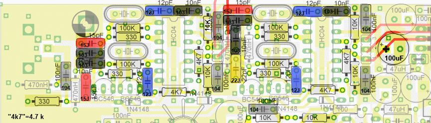
It is a good idea to keep a small separation between the bottom of the crystal and the top of the board when installing the crystals. One way to do this is to insert a tiny piece of folded paper underneath the crystal to act as a separator "shim".
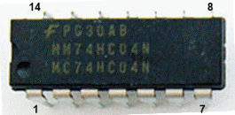
When installing the 74HC04N ICs, pay close attention to their orientation. The end with the dimple corresponds to the silkscreen end with a notch in it. Pin 1 of the IC is as indicated in the graphic on the bill of materials.
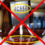
Be careful not to confuse the BC5
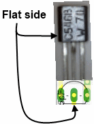
Note the orientation of the transistors on the board: they are mounted such that the flat side of the transistor is aligned with the flat dimension of the silkscreened layout for the transistor and, again, be sure to mount the correct transistor (BC546, not BC556):
| Check | Designation | Component | Marking | Category | Orientation | Notes |
|---|---|---|---|---|---|---|
| ❏ | U2-1 | 74HC04 Hex Inverter |
| DIP-14 | Take ESD precautions | |
| ❏ | U2-2 | 74HC04 Hex Inverter |
| DIP-14 | Take ESD precautions | |
| ❏ | Q2-1 | BC546 NPN Transistor |
| TO-92 | ||
| ❏ | Q2-2 | BC546 NPN Transistor |
| TO-92 | ||
| ❏ | Q2-3 | BC546 NPN Transistor |
| TO-92 | ||
| ❏ | Q2-4 | BC546 NPN Transistor |
| TO-92 | ||
| ❏ | X2-1 | 40.500 MHz HC48S Crystal |
| Xtal | ||
| ❏ | X2-2 | 56.180 MHz HC48S Crystal |
| Xtal | ||
| ❏ | X2-3 | 56.552 MHz HC48S Crystal |
| Xtal | ||
| ❏ | X2-4 | 56.928 MHz HC48S Crystal |
| Xtal |
Inspect Completed Board
Visually inspect the board, paying close attention to the following, which have caused problems for some builders:
- Inductors (all four must be 470 nH yellow-biolet-silver-gold)
- ICs (both must be 74HC04)
- Transistors (all four must be BC546, not BC556) and oriented with their flat sides toward the bottom edge of the board.
- Diodes: of the four 1N4148s, three are oriented with their bands on the LEFT and one has the band on the RIGHT)
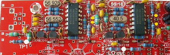
- Crystals: separated slightly from the board and in the correct positions (per the layout diagram). Note that, just in the photo below, one crystal was not available for installatin at the time the photo was taken. You should have all four crystals installed.
- Capacitors: double check the band-specific capacitors for correct values and placement (i.e., the values in addition to the customary 103 and 104 capacitors)
- Resistors: recall from above that there are three "opportunities for mischief" in this stage, whereby the builder solders one lead of a resistor into a square hole instead of a round hole. Carefully check each of those locations and be sure you got it right.
- Inspect the underside for solder bridges, cold joints, etc.
Local Oscillators Testing
Oscillator Output Tests
Test Setup
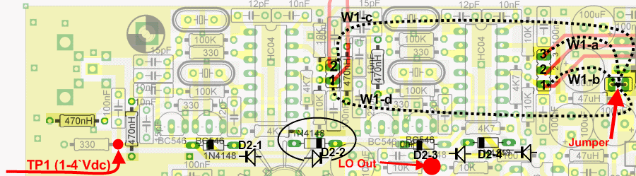
The first oscillator to check is one for 30m band which resonates at 40500 kHz.
1. solder temporary wire (as "W1-a") between jumper JK1 and JP1 pin 3. (You may prefer to use a wire with test clips on either end as Wire1 (rather than soldering and unsoldering).
2. check the voltage at test point TP1 with digital multi meter. It should read around +2V. If the test voltage is 0V or 5V then oscillator is not oscillating.
3. in same way test three remaining oscillators by connecting W1 wire:
- As "W1-b" to points JP1 pin 1 (56.180MHz)
- As "W1-c" to JP2 pin 2 (56.552MHz) and
- As "W1-d" to JP2 pin 1 (56.928MHz)
(In the dividers stage, we will check the oscillator's functionality again, but at frequencies sensible to the average HF RX)
Some builders have had difficulties getting the 30m Oscillator to work. If this is your case, check out message 1467 in the Yahoo Group, calling for replacing the 22pF capacitor with a 27pF capacitor.
Test Measurements
| Testpoint | Units | Nominal Value | Author's | Yours |
|---|---|---|---|---|
| 40.5MHz (10.125): W1=JK1-JP1-3 (TestPoint TP1) | Vdc | +2 | 3.382 | _______ |
| 56.18MHz (14.045): W1=JK1-JP1-1 (TestPoint TP1) | Vdc | +2 | 3.374 | _______ |
| 56.552MHz (14.138): W1=JK1-JP2-2 (TestPoint TP1) | Vdc | +2 | 3.382 | _______ |
| 56.928MHz (14.232): W1=JK1-JP2-1 (TestPoint TP1) | Vdc | +2 | 3.431 | _______ |
| LO Out (junction of 2 10k resistors - voltage divider) | Vdc | +2.5 | 2.51 | _______ |
Frequency Output
Test Setup
If you have a frequency counter or scope, connect each of the four oscillators, in turn, and look for a signals to verify that the oscillator is providing output.
You can probe at the "LO Out" testpoint (see above) for the desired signal.Test Measurements
| Testpoint | Units | Nominal Value | Author's | Yours |
|---|---|---|---|---|
| LO Out: 40.5 MHz selected | MHz | 40.5 | 40.5 | _______ |
| LO Out: 56.18 MHz selected | MHz | 56.18 | 56.18 | _______ |
| LO Out: 56.552 MHz selected | MHz | 56.552 | 56.55 | _______ |
| LO Out: 56.928 MHz selected | MHz | 56.928 | 56.93 | _______ |