TX Driver and PA Introduction
General
Here is a Youtube Video of Dragan 4O4A's QSO with his completed G3020. Plough through this last stage and you can be there, too!
NB: If you Plan to Use the Transceiver for Digital Modes
From the Preston Smith's (WJ2V) FAQ on the GenesisRadio web site:
Q: My final PA gets hot/blew out while transmitting in digital mode. What happened?
A: The Genesis is suppled with a 1" heat sink for the final. This is adequate for casual SSB or CW operating, but not for digital (e.g. PSK31, SSTV, WSPR) modes, which are much more demanding. Linear key-down modes require a larger heat sink, and a fan to protect the final PA, an IRF 510.
If you blow one, you can buy a replacement for about two dollars at Radio Shack. You can find a direct fit, only taller, replacement heat sink at Digikey: 2" and a 2.5" heatsinks have Digikey part numbers: HS287-ND and HS133-P-ND, respectively.
Either should work, but also consider a small fan on top for long key down or contest modes.
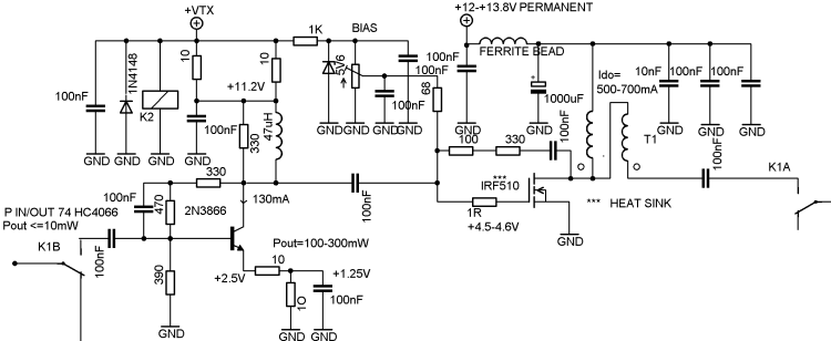
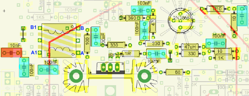
(go directly to build notes)TX Driver and PA Schematic
(go directly to build notes)
TX Driver and PA Bill of Materials
Stage Bill of Materials
(resistor images and color codes courtesy of WIlfried, DL5SWB's R-Color Code program)
| Check | Count | Component | Marking | Category |
|---|---|---|---|---|
| ❏ | 1 | 1 k 1/4W 1% | br-blk-blk-br-br
 | 1/4W |
| ❏ | 3 | 10 ohm 1/4W 1% | br-blk-blk-gld-br
 | 1/4W |
| ❏ | 1 | 100 1/4W 1% | br-blk-blk-blk-br
 | 1/4W |
| ❏ | 1 | 1R 1/4W 1% (1R) | brn-blk-blk-silver-brn
 | 1/4W |
| ❏ | 3 | 330 1/4W 1% | ora-ora-blk-blk-brn
 | 1/4W |
| ❏ | 1 | 390 1/4W 1% | ora-whi-blk-blk-brn
 | 1/4W |
| ❏ | 1 | 470 1/4W 1% | yel-vio-blk-blk-brn
 | 1/4W |
| ❏ | 1 | 68.0 1/4W 1% | blu-gry-blk-gld-brn
 | 1/4W |
| ❏ | 2 | BN43-202 |
 | Binocular core |
| ❏ | 1 | 10 nF (.01uF) | 103
 | Ceramic |
| ❏ | 1 | 100 nF | 104
 | Ceramic |
| ❏ | 3 | 100 nF | 104
| Ceramic |
| ❏ | 4 | 100 nF | 104
| Ceramic |
| ❏ | 1 | 47 uH molded inductor 10% | yel-vio-blk-slv
 | Choke |
| ❏ | 2 | shunt wire (cut-off lead) | Cutoff | |
| ❏ | 1 | M3 screw and nut set | HDW | |
| ❏ | 1 | Magnet wire, enameled #20 | Magnetic | |
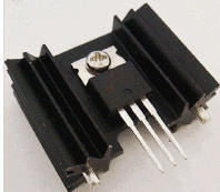
| ❏ | 1 | TO-220 1" Heatsink |
 | Misc |
| ❏ | 1 | TO-39 heatsink |
 | Misc |
| ❏ | 1 | SPDT 2 position | SPDT | |
| ❏ | 1 | SPDT 2 position | SPDT | |
| ❏ | 1 | SPDT 2 position | SPDT | |
| ❏ | 1 | Power MOSFET IRF510 | IRF510
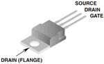 | TO-220 |
| ❏ | 1 | 2N3866 NPN Transistor |
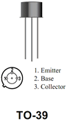 | TO-39 |
TX Driver and PA Summary Build Notes
- Install Driver Transistor and Heat Sink
- Wind and Install the Dual Binocular Transformer
- Install Passive Components
- Install the 2 Jump Wires
- Install PA FET and Heat Sink
- Install Remaining Wires
- Install Remaining Switches
- Test the Stage
TX Driver and PA Detailed Build Notes
Top of the Board
Install Driver Transistor and Heat Sink
Install the 2N3866 transistor and its heatsink. Refer to the instructions in Phase 6 for details on mounting and installing the 2N3866.
| Check | Designation | Component | Marking | Category | Orientation | Notes |
|---|---|---|---|---|---|---|
| ❏ | misc10-2 | TO-39 heatsink |
| Misc | ||
| ❏ | Q10-2 | 2N3866 NPN Transistor |
| TO-39 |
Wind and Install the Dual Binocular Transformer
Glue together the two binary cores as indicated in the graphic, below:

Take care when gluing the two cores together to carefully set and align them so they are aligned with one another, as in the image. There is a tendency, especially when using "Super Glue" to let them slide out of aligment just as the glue sets, making recovery and realignment quite difficult.
Twisted Wire
Prepare a 40 cm (~16") long piece of enameled copper wire and fold it over so that it is two 20 cm wires joined at the one end
Twist the wires together so that you get approximately three twists per 10 mm (3 twists per every 0.4 inches) of length
Wind the Wire through the Core
Click Picture to Enlarge

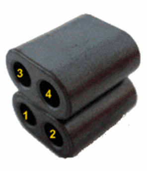
Thread the twisted wires (folded end first) through the glued cores, starting in hole 1, coming out the other end and looping back through the top core to exit at hole 3. Continue from hole 3 into hole 2, coming out the other end and looping back into the upper core so as to exit at hole 4.
When finished winding, cut the folded end of the twisted wire off, such that you noe have four wire ends.
The pair at hole 1 represents the primary leads; the pair at hole 4 represents the secondary leads of the wound transformer.
Using an ohm meter, identify the ends of each wire as indicated on the graphic above. You may want to use a small piece of colored hookup wire insulation to identify the "a-a1" pair (or, if you prefer, the "b-b1 pair") wire's ends.
Mount the Transformer
You do not need to worry how to figure out the phasing; if you match the designated leads (a1, b1, a, b) with the holes as marked in the graphic below, you will have correct phasing.


Insert transformer's leads into the PCB holes, as indicated above. Form the leads and pull them tight. Then cut off the excess (on the underside of the board) so that approximately 5mm (1/8") of wire is protruding out on the underside of the board.
Remove the transformer from the PCB, scrape the enamel coating from the 4 leads but DO NOT TIN them as yet (tinning the leads could cause them to be too "fat" to go back into the holes).
Insert the 4 transformer leads back into the PCB and solder them.
| Check | Designation | Component | Marking | Category | Orientation | Notes |
|---|---|---|---|---|---|---|
| ❏ | misc10-1 | Magnet wire, enameled #20 | Magnetic |
Install Passive Components
Install resistors, capacitors, chokes
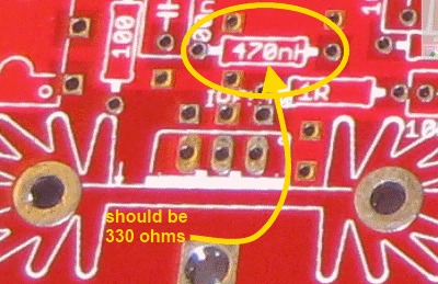
Some PCBs for the G3020 have a silkscreen image suggesting that the component to be installed just above the 1 ohm ("1R") resistor is a 470 nH inductor. The silkscreen is incorrect. It should be a 330 ohm resistor, NOT an inductor. See the top of the board graphic - it is correct.
| Check | Designation | Component | Marking | Category | Orientation | Notes |
|---|---|---|---|---|---|---|
| ❏ | C10-8 | 10 nF (.01uF) | 103
| Ceramic | (added) | |
| ❏ | R10-1 | 1R 1/4W 1% (1R) | brn-blk-blk-silver-brn
| 1/4W | ||
| ❏ | R10-2 | 10 ohm 1/4W 1% | br-blk-blk-gld-br
| 1/4W | ||
| ❏ | R10-3 | 10 ohm 1/4W 1% | br-blk-blk-gld-br
| 1/4W | ||
| ❏ | R10-4 | 10 ohm 1/4W 1% | br-blk-blk-gld-br
| 1/4W | ||
| ❏ | R10-5 | 68.0 1/4W 1% | blu-gry-blk-gld-brn
| 1/4W | ||
| ❏ | R10-6 | 100 1/4W 1% | br-blk-blk-blk-br
| 1/4W | ||
| ❏ | R10-7 | 330 1/4W 1% | ora-ora-blk-blk-brn
| 1/4W | ||
| ❏ | R10-8 | 330 1/4W 1% | ora-ora-blk-blk-brn
| 1/4W | ||
| ❏ | R10-9 | 330 1/4W 1% | ora-ora-blk-blk-brn
| 1/4W | ||
| ❏ | R10-10 | 390 1/4W 1% | ora-whi-blk-blk-brn
| 1/4W | ||
| ❏ | R10-11 | 470 1/4W 1% | yel-vio-blk-blk-brn
| 1/4W | Note: This is a 470R, NOT a 4k7 or 47k. | |
| ❏ | R10-12 | 1 k 1/4W 1% | br-blk-blk-br-br
| 1/4W | (reloc) | |
| ❏ | C10-1 | 100 nF | 104
| Ceramic | ||
| ❏ | C10-2 | 100 nF | 104
| Ceramic | ||
| ❏ | C10-3 | 100 nF | 104
| Ceramic | ||
| ❏ | C10-4 | 100 nF | 104
| Ceramic | ||
| ❏ | C10-5 | 100 nF | 104
| Ceramic | (reloc) | |
| ❏ | C10-6 | 100 nF | 104
| Ceramic | (reloc) | |
| ❏ | C10-7 | 100 nF | 104
| Ceramic | (reloc) | |
| ❏ | R10-12 | 100 nF | 104
| Ceramic | (reloc) | |
| ❏ | L10-3 | 47 uH molded inductor 10% | yel-vio-blk-slv
| Choke |
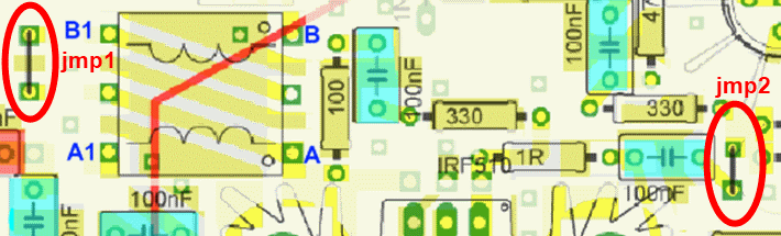
Install the 2 Jump Wires
| Check | Designation | Component | Marking | Category | Orientation | Notes |
|---|---|---|---|---|---|---|
| ❏ | JMP10-1 | shunt wire (cut-off lead) | Cutoff | |||
| ❏ | JMP10-2 | shunt wire (cut-off lead) | Cutoff |
Install PA FET and Heat Sink
Be sure the transistor is oriented with its flat "Drain Flange" (see BOM for the final transistor) facing the bottom of the board.
| Check | Designation | Component | Marking | Category | Orientation | Notes |
|---|---|---|---|---|---|---|
| ❏ | Q10-1 | Power MOSFET IRF510 | IRF510
| TO-220 | ||
| ❏ | hdw10-1 | M3 screw and nut set | HDW | |||
| ❏ | misc10-1 | TO-220 1" Heatsink |
| Misc |
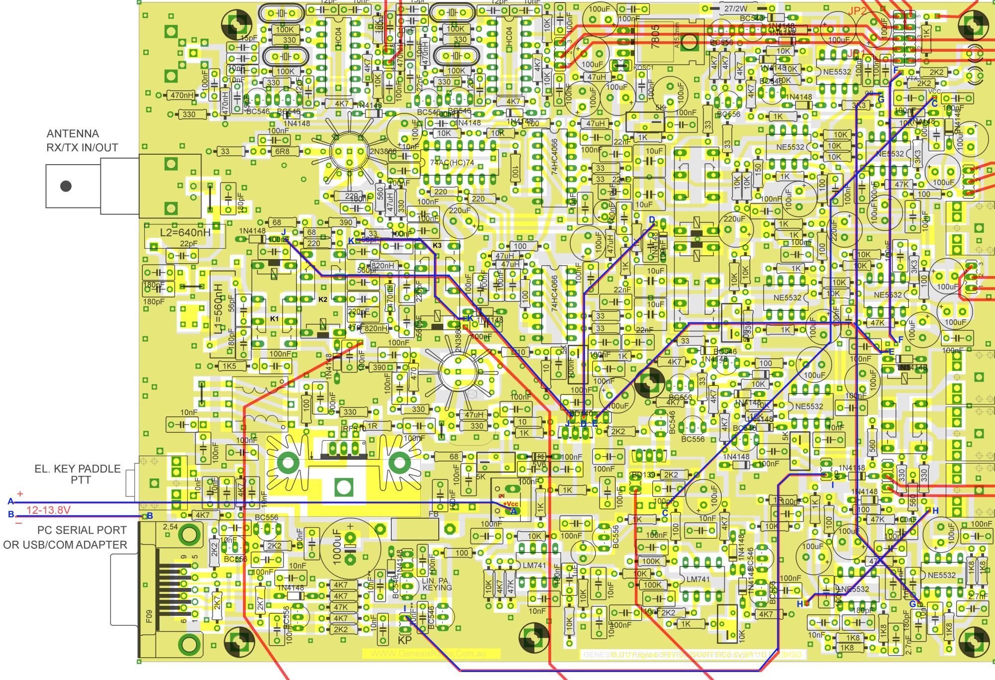
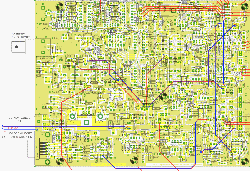
Install Remaining Wires
Install the remaining permanent wires to the board. Some have been already installed in previous phases. At this point, if you have not removed any temporary wires/switches, you should do so now. For your help in this effort, all permanent (non-switch associated) wires are itemized in the following table:
| Check | Designation | Component | Marking | Category | Orientation | Notes |
|---|---|---|---|---|---|---|
| ❏ | Wires A-A and B-B | Misc Hookup Wire | Final Permanent Wires | Vcc Connection (Phase 8) | ||
| ❏ | Wire C-C | Misc Hookup Wire | Final Permanent Wires | W9 (Phase 9) | ||
| ❏ | Wire D-D | Misc Hookup Wire | Final Permanent Wires | This Phase | ||
| ❏ | Wire E-E | Misc Hookup Wire | Final Permanent Wires | This Phase | ||
| ❏ | Wire F-F | Misc Hookup Wire | Final Permanent Wires | This Phase | ||
| ❏ | Wire G-G | Misc Hookup Wire | Final Permanent Wires | W8 (Phase 9) | ||
| ❏ | Wire H-H | Misc Hookup Wire | Final Permanent Wires | W4 (Phase 7) | ||
| ❏ | Wire I-I | Misc Hookup Wire | Final Permanent Wires | This Phase | ||
| ❏ | Wire J-J | Misc Hookup Wire | Final Permanent Wires | This Phase | ||
| ❏ | Wire K-K | Misc Hookup Wire | Final Permanent Wires | W3 (Phase 6) |
Click to see a high resolution picture of the wires.
Install Remaining Switches
If, at this point, you have not removed any temporary switches, you should do so and then ensure you have all of the permanent switches.
Some builders may have postponed the actual wiring and installation of switches in earlier stages, in order to make handling of the board less complicated. If this is the case, those switches must be installed at this point and it would be a good idea to review any tests associated with the switches with a view toware repeating the tests.
Note that there were two options to handling the band-switching of the oscillator's crystals: the original design, using the panel, LEDs, and DPDT switches; and the use of the Rotary Switch with no LEDs. It is your decision.
Refer to the Final Diagram for the final positioning and wiring of all of the Switches
Watch out for the pre-amp and attenuator switches in the Final Diagram. In the lower right hand corner there are they are labeled PREAMP and ATTN. According to the wiring of these two switches in the diagram, the names on the two switches have been reversed. The upper switch should be labeled ATTN and the lower switch should be labeled PREAMP.
The table below provides information on the switches, their function, and the stage withn which they were described/defined/installed:
| Check | Switch | Function | Stage in Which Defined |
|---|---|---|---|
| ❏ | BandSwitch | Switches one of 4 crystals into LO | Band Switch |
| ❏ | AF Gain Switch (SW10-1) | Selects 23dB or 46dB gain on RX I and Q to PC | RX Mixers/OpAmps |
| ❏ | RF Preamp (SW10-2) | Switches +15 dB PreAmp into or out of RF path | LP Filters and PreAmp |
| ❏ | RF Attenuator (SW10-3) | Switches -17dB RF Attenuator into RF path | LP Filters and PreAmp |
| ❏ | Monitor Switch | CW/SSB Digital CW Monitor On/Off | CW Monitor |
| Check | Designation | Component | Marking | Category | Orientation | Notes |
|---|---|---|---|---|---|---|
| ❏ | SW10-1 | SPDT 2 position | SPDT | AF Gain 23dB/46dB | ||
| ❏ | SW10-2 | SPDT 2 position | SPDT | RF Pre-Amp | ||
| ❏ | SW10-3 | SPDT 2 position | SPDT | RF Attenuator |
TX Driver and PA Testing
Finals Resistance Tests
Test Setup
with power off, measure:
- Resistance from source to gate of the IRF10 MOSFET Final Amplifier. Should be greater than 1.2k ohms (in the range of 1.3k-1.6k)
- Resistance from source to drain (in the same range, but rising to eventually over 7k ohms)
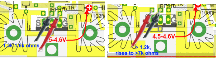
Test Measurements
| Testpoint | Units | Nominal Value | Author's | Yours |
|---|---|---|---|---|
| IRF10 PA source-to-gate resistance | k ohm | 1.3 - 1.6 | tbd | _______ |
| IRF10 PA source-to-drain resistance | k ohm | 1.3 rise to > 7 | tbd | _______ |
Driver Voltage Test
Test Setup
While transmitting, measure the voltage at the emitter of the 2N3866 driver transistor. It should be +/- 2.5vdc.
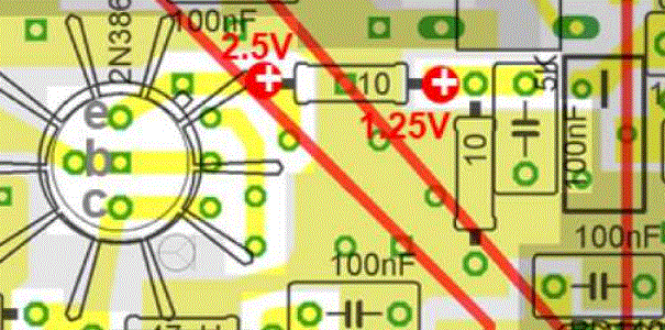
Test Measurements
| Testpoint | Units | Nominal Value | Author's | Yours |
|---|---|---|---|---|
| Emitter of driver transistor | Vdc | 2.5 | tbd | _______ |